Download
1 / 15
150 likes | 162 Views
DEPFET Thinning Technology - Experiences and First Results -. L. Andricek a , P.Fischer b , G.Lutz a , R.H.Richter a , M.Schumacher c , M.Trimpl c , J.Ulrici c , N.Wermes c. Introduction - Module Concept Technology Overview Direct Wafer Bonding Deep Etching

E N D
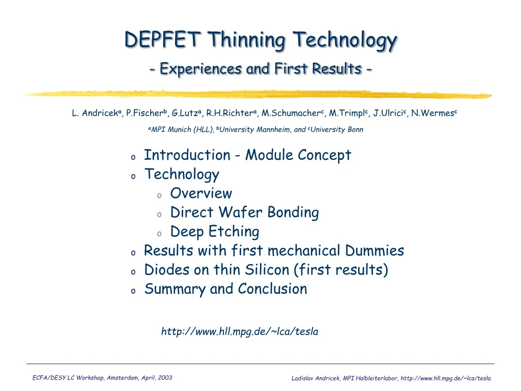
DEPFET Thinning Technology- Experiences and First Results - L. Andriceka, P.Fischerb, G.Lutza, R.H.Richtera, M.Schumacherc, M.Trimplc, J.Ulricic, N.Wermesc • Introduction - Module Concept • Technology • Overview • Direct Wafer Bonding • Deep Etching • Results with first mechanical Dummies • Diodes on thin Silicon (first results) • Summary and Conclusion http://www.hll.mpg.de/~lca/tesla aMPI Munich (HLL), bUniversity Mannheim, and cUniversity Bonn Ladislav Andricek, MPI Halbleiterlabor, http://www.hll.mpg.de/~lca/tesla
readout chips reduce frame material!!! by etching of "holes" in the frame readout chips perforated frame: 0.05 % X0 total: 0.11 % X0 Module Concept 5-layer (CCD-like) layout for the vertex detector 1st layer module: sensitive area 100x13 mm2 sensitive area thinned down to 50 mm, supported by a directly bonded 300 mm thick frame of silicon Estimated Material Budget (1st layer): Pixel area: 100x13 mm2, 50 mm : 0.05% X0 steer. chips: 100x2 mm2, 50 mm : 0.008% X0 (massive) Frame :100x4 mm2, 300 mm : 0.09% X0 Ladislav Andricek, MPI Halbleiterlabor, http://www.hll.mpg.de/~lca/tesla
a) oxidation and back side implant of top wafer c) process passivation Top Wafer Handle <100> Wafer open backside passivation b) wafer bonding and grinding/polishing of top wafer d) anisotropic deep etching opens "windows" in handle wafer Processing thin detectors- the Idea - Ladislav Andricek, MPI Halbleiterlabor, http://www.hll.mpg.de/~lca/tesla
Processing thin detectors- Direct Wafer Bonding - “SOI” Wafer prepared by MPI für Microstrukturphysik, Halle ≈1 cm/sec picture from: www.mpi-halle.mpg.de Q.-Y. Tong and U. Gösele “ Semiconductor Wafer Bonding ” John Wiley & Sons, Inc. Ladislav Andricek, MPI Halbleiterlabor, http://www.hll.mpg.de/~lca/tesla
Processing thin detectors- anisotropic wet etching - Hydroxide etching of silicon: KOH, NaOH, … , TMAH: (CH3)4 NOH 54.72 deg Ladislav Andricek, MPI Halbleiterlabor, http://www.hll.mpg.de/~lca/tesla
good selectivity to oxide almost perfect selectivity to Al no alkali ions poorer selectivity to (111) (≈30:1) rough surface after etching (hillocks) Etch solution: 5 wt.% TMAH 1.6 wt.% dissolved silicon 0.4 wt.% (NH4)2S2O8 -> at 80 – 85 ºC forms a passivation layer on Aluminium pads: Aluminium-oxide Aluminium silcates { } Processing thin detectors - anisotropic wet etching - Tetra-Methyl-Ammonium-Hydroxide Ladislav Andricek, MPI Halbleiterlabor, http://www.hll.mpg.de/~lca/tesla
Processing thin detectors- open questions/possible problems - How thin can we get? How good/reliable is wafer bonding? How good/reliable is etching with TMAH? Are these custom made "SOI" wafers good enough for high quality/low noise pixel sensors? Does the thinning procedure affect the sensor performance? Ladislav Andricek, MPI Halbleiterlabor, http://www.hll.mpg.de/~lca/tesla
principle works!! 50 mm seems to be a reasonable thickness diced samples robust enough for safe handling 26 μm 51 μm Mechanical Dummies - distortions - window dimensions: (50x13)/4 mm2 6.5x6.5 mm2 80x10.4 mm2 (80% of tesla sensor) (50x13)/2 mm2 50x13 mm2 10 "SOI" wafers with top layer different thickness 24 - 29 micron (3 Wafers) 36 - 38 micron (3 Wafers) 43 - 51 micron (4 Wafers) Etched with KOH at CiS Erfurt Ladislav Andricek, MPI Halbleiterlabor, http://www.hll.mpg.de/~lca/tesla
p+ SiO2 Type I: Simplified standard technology Type II: Implants like DEPFET config. Al n+ n+ SiO2 p+ structured p+ on top unstructured n+ in bond region 3 Wafers unstructured n+ on top structured p+ in bond region 3 Wafers Al Diodes & Teststructures on thin Silicon * test bondability of implanted oxide & electrical performance of diodes on thin silicon * 2 types of thinned diodes * + 4 Wafers with standard Diodes as a reference * Ladislav Andricek, MPI Halbleiterlabor, http://www.hll.mpg.de/~lca/tesla
Type II: pn-junction in bond region etched rectangles for material reduction in the frame Diodes & Teststructures on thin Silicon Type I: pn-junction on top wafer surface white areas will be thinned to 50 μm after processing Ladislav Andricek, MPI Halbleiterlabor, http://www.hll.mpg.de/~lca/tesla
Direct Wafer Bonding possible, but some voids after annealing! improve surface condition before bonding Diodes & Teststructures on thin Silicon- Direct Wafer bonding after Implantation - Bonded wafers (structured implant through BOX): infrared transmission pictures from MPI Halle (M. Reiche) Ladislav Andricek, MPI Halbleiterlabor, http://www.hll.mpg.de/~lca/tesla
50 mm, standard diode, 10 mm2 250 mm, standard diode, 10 mm2 C(Vfd) t = 46 mm Diodes & Teststructures on thin Silicon- Type I: CV curves, full depletion voltage - handle wafer not yet etched!!! Ladislav Andricek, MPI Halbleiterlabor, http://www.hll.mpg.de/~lca/tesla
250 mm, 4 standard diodes, 10 mm2 50 mm, 4 standard diodes, 10 mm2 Diodes & Teststructures on thin Silicon- Type I: IV curves - handle wafer not yet etched!!! Reverse currents almost the same for both wafer types (about 1 nA/cm2) !!!??? Stress in the bond interface???? process related??? …??? more investigations in the next weeks Ladislav Andricek, MPI Halbleiterlabor, http://www.hll.mpg.de/~lca/tesla
Diodes & Teststructures on thin Silicon- Type II: results of the test etching - partially etched: Si rest on SiO2 study: octagonal "honeycomb" Ladislav Andricek, MPI Halbleiterlabor, http://www.hll.mpg.de/~lca/tesla
DEPFET Thinning Technology- Summary and Conclusions - • A module concept for the 1st layer of the TESLA vertex detector was presented. • The sensitive pixel area thinned down to 50 mm and supported by an integrated silicon frame. • Perforating the frame reduces the contribution to the material budget to 0.11% X0 for the first layer. • The feasibility of the thinning technology was shown: • 50 mm thickness in the sensitive area is easily achievable. • Direct wafer bonding with implanted and structured interface is possible, (optimizations concerning the density of voids) • TMAH (with the appropriate additives) seems to be a good choice for the deep etching • First IV measurements of diodes on thin silicon are extremely encouraging: reverse current < 1 nA/cm2. Next steps: Continue etching next week, more IV/CV measurements, dicing of the "chips" and more detailed mechanical investigations……. Ladislav Andricek, MPI Halbleiterlabor, http://www.hll.mpg.de/~lca/tesla