Download
1 / 21
210 likes | 300 Views
Project Status. Growing # of Applications for SERDES PCI Card Available SERDES based PLD Devices Status of Development Cards Status of QIE Readout Cards for Test beam Simulation Results of TDC w/ 400ps Resolution Discussed at San Luis Potosi Workshop. Applications for Serdes PCI Design.

E N D
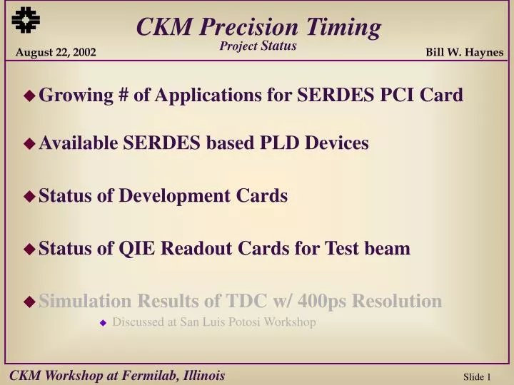
Project Status • Growing # of Applications for SERDES PCI Card • Available SERDES based PLD Devices • Status of Development Cards • Status of QIE Readout Cards for Test beam • Simulation Results of TDC w/ 400ps Resolution • Discussed at San Luis Potosi Workshop
Applications forSerdesPCI Design • Time to Digital Converter (TDC) • Timing Distribution System (TDS) • Mesh Network for Lattice Gauge PC Farm • ReProgrammable data link like the QIE readout Card • Other Applications w/ PLD Based SERDES Devices?
Available SERDES Based PLD Devices • Orca ORT82G5 from Lattice • 8-channel 3.5 Gbs SERDES • In production & Cost is ~$300 • 20-channel 3.5 Gbs SERDES in development • Xilinx-II Pro FPGA • 4-channel 3.125 Gbs SERDES • In production & Cost is ~$300 • 16-channel 3.125 Gbs SERDES in development • Altera Stratix FPGA • EP1S25 780-pin w/ 58-channels of LVDS @ 840 Mbs • In production & Cost is ~$800 • EP1S25 1020-pin w/ 78-channels of LVDS @ 840 Mbs • In production & Cost is ~$1500 • EP1S40 1020-pin w/ 80-channels of LVDS @ 840 Mbs • Available next month & Cost is ~$UNK • Cypress Programmable Serial Interface (PSI) • CPLD w/ a dual channel 2.5Gbs SERDES device • Discontinued
TDC Based on a SERDES PLD Devices General I/O 156 MHz Ref Clk ORCA/Xilinx FPGA 16bit Data Optical or CML From Detector Serial Receiver PCI Bus FPGA Serdes Control Notes: 1.)The SERDES receiver must be capable of locking to the reference clock. 2.) The 8b10b encoder of the receiver must be capable of being by-passed. General I/O Simplified TDC Block Diagram
PCI Cards with TDC functionality • 8 channel Orca ORT82G5 w/ 3.5 Gbs SERDES • Resolution is ~285ps • Status: In final stages of artwork layout • 80 channel 840 Mbs links (LVDS), Altera Stratix EPS25 or EPS40 • Resolution is ~1.2ns • Status: Artwork layout will start in earily September, 2002 • 4 channel Xilinx XC2VP4 Virtex-II Pro w/ 3.125 Gbs SERDES • Resolution is ~320ps • Status: will start layout when Orca layout is complete
Our First Serdes Based Design • PCI Card w/ two 2.5Gbs TI Serial Links (CoLink) • One Differential Copper Link • One Optical Link • Designed May 30, 2000
QIE Readout Card • QIE Readout Card is a Modified CoLink Card
QIE Readout Card • QIE Readout Card (QIElink) • One Optical Link @ 700 Mbs • Input circular buffer (2K x 16bit) • Stores up to the last 2K words of QIE data prior to a NIM stop • Nim Stop Input • Inhibits additional circular buffer writing of QIE data • Sets CSR register bit for PCI readout of QIE data • Current Status for Fall Test Beam • Four cards assembled and tested • Cards were tested in pairs • One to generate QIE data and a NIM stop • The other to store the QIE data and trigger a PCI readout • PCI driver for Windows and Linux is complete • See Dave Slimmer for details
TDC w/ 400ps Resolution • Input Pulse Width = FFFF F800 0000-> 21bits x 6.4ns/16 = 21 x 400ps = 8.4ns • Reference Counter Time = T Ref = 105.6ns • T Ref Offset = # of 0 bits from T Ref x 400ps = 0 x 400ps = 0ps • Input Prop. Delay = 29.200075ns + T Ref Offset = 29.200075ns 105.6ns FFFF
TDC w/ 400ps Resolution • Input Pulse Width = 7FFF FC00 0000-> 21bits x 6.4ns/16 = 21 x 400ps = 8.4ns • Reference Counter Time = T Ref = 105.6ns • T Ref Offset = # of 0 bits from T Ref x 400ps = 1 x 400ps = 400ps • Input Prop. Delay = 28.800075ns + T Ref Offset = 28.800075ns +400ps = 29.200075ns 105.6ns 7FFF
TDC w/ 400ps Resolution • Input Pulse Width = 3FFF FE00 0000-> 21bits x 6.4ns/16 = 21 x 400ps = 8.4ns • Reference Counter Time = T Ref = 105.6ns • T Ref Offset = # of 0 bits from T Ref x 400ps = 2 x 400ps = 800ps • Input Prop. Delay = 28.400075ns + T Ref Offset = 28.400075ns +800ps = 29.200075ns 105.6ns 3FFF
TDC w/ 400ps Resolution • Input Pulse Width = 0FFF FF80 0000-> 21bits x 6.4ns/16 = 21 x 400ps = 8.4ns • Reference Counter Time = T Ref = 105.6ns • T Ref Offset = # of 0 bits from T Ref x 400ps = 4 x 400ps = 1600ps • Input Prop. Delay = 27.600075ns + T Ref Offset = 27.600075ns +1600ps = 29.200075ns 105.6ns 0FFF
TDC w/ 400ps Resolution • Input Pulse Width = 0001 FFFFF000-> 21bits x 6.4ns/16 = 21 x 400ps = 8.4ns • Reference Counter Time = T Ref = 105.6ns • T Ref Offset = # of 0 bits from T Ref x 400ps = 15 x 400ps = 6000ps • Input Prop. Delay = 23.200075ns + T Ref Offset = 23.200075ns +6000ps = 29.200075ns 105.6ns 0001
TDC w/ 400ps Resolution • Input Pulse Width = 0000 FFFFF800-> 21bits x 6.4ns/16 = 21 x 400ps = 8.4ns • Reference Counter Time = T Ref = 105.6ns + 6.4ns = 112.0 ns • T Ref Offset = # of 0 bits from T Ref x 400ps = 0 x 400ps = 0ps • Input Prop. Delay = 29.200075ns + T Ref Offset = 29.200075ns +0ps = 29.200075ns 112.0ns FFFF
TDC w/ 400ps Resolution • Input Pulse Width = 0000 0FFE0000-> 11bits x 6.4ns/16 = 11 x 400ps = 4.4ns +/-200ps • Reference Counter Time = T Ref = 105.6ns + 0ns = 105.6 ns • T Ref Offset = # of 0 bits from T Ref x 400ps = 4 x 400ps = 1600ps • Input Prop. Delay = 27.600075ns + T Ref Offset = 27.600075ns +1600ps = 29.200075ns 105.6ns 0FFE
TDC w/ 400ps Resolution • Input Pulse Width = 0000 0E000000-> 3bits x 6.4ns/16 = 3 x 400ps = 1.2ns +/-200ps • Reference Counter Time = T Ref = 105.6ns + 0ns = 105.6 ns • T Ref Offset = # of 0 bits from T Ref x 400ps = 4 x 400ps = 1600ps • Input Prop. Delay = 27.600075ns + T Ref Offset = 27.600075ns +1600ps = 29.200075ns 105.6ns 0E00 1.0ns
TDC w/ 400ps Resolution • Input Pulse Width = 0000 08000000-> 1bits x 6.4ns/16 = 1 x 400ps = 400ps +/-200ps • Reference Counter Time = T Ref = 105.6ns + 0ns = 105.6 ns • T Ref Offset = # of 0 bits from T Ref x 400ps = 4 x 400ps = 1600ps • Input Prop. Delay = 27.600075ns + T Ref Offset = 27.600075ns +1600ps = 29.200075ns 105.6ns 0800 400ps
Timing (or Clock) Distribution System (TDS) • The Far-End of the Cable is a Common Reference for all Receivers • Reference can be Determined by: T = (Round Trip Time)/2 Or • The Time from Incident Wave to the Reflected Wave Divided by Two TfarEnd= (TI-Wave – TR-Wave)/2 R-Wave I-Wave TfarEnd= (TI-Wave – TR-Wave)/2 R-Wave Round Trip Time = 2T I-Wave R-Wave I-Wave TfarEnd= (TI-Wave – TR-Wave)/2