Download
1 / 56
570 likes | 777 Views
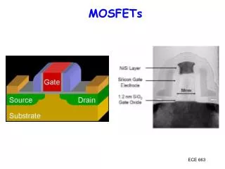
Chap.1 Physics and Modelling of MOSFETs. 반도체 연구실 신입생 세미나 박 장 표 2009 년 1 월 8 일. Contents. Basic MOSFET Characteristics Current – Voltage Characteristics p-Channel MOSFETs Geometric Scaling Theory Small – Device Effects Small Device Model. 2.

E N D
Chap.1 Physics and Modelling of MOSFETs 반도체 연구실 신입생 세미나 박 장 표 2009 년 1 월 8 일
Contents • Basic MOSFET Characteristics • Current – Voltage Characteristics • p-Channel MOSFETs • Geometric Scaling Theory • Small – Device Effects • Small Device Model 2
1.1 Basic MOSFET Characteristics • The MOS Threshold Voltage • Body Bias 3
Basic MOSFET Characteristics • MOSFET used as a Switch • ID determine by VGS &VDS ( also VSB affects lesser degree ) 4
Basic MOSFET Characteristics • W, L are important dimension for electrical characteristics • Aspect ratio : W / L 5
Basic MOSFET Characteristics • The MOS Threshold Voltage : used to enhance the conduction between the drain and source • VGS < VT : cutoff ( no current flow - ideally ) , VGS > VT : active mode • ID depends on the voltages applied 6
Basic MOSFET Characteristics • MOS system : altering the charge distribution at the surface 7
Basic MOSFET Characteristics For small values of VG • Create depletion region referred to as bulk charge • The surface charge is made up entirely of bulk charge • Bulk charge consists of ionized acceptor atom, it is immobile 8
Basic MOSFET Characteristics For VG > VT • initiates thin electron inversion layer when VG = VT 9
Basic MOSFET Characteristics • The MOS Threshold Voltage 10
Basic MOSFET Characteristics • Body Bias 11
1.2 Current – Voltage Characteristics • Square-Law Model • Bulk-Charge Model 12
Current – Voltage Characteristics • Cutoff when VGS < VT 13
Current – Voltage Characteristics • Active when VGS > VT 14
Current – Voltage Characteristics • Square-Law Model 15
Current – Voltage Characteristics • Channel Length Modulation 16
Current – Voltage Characteristics • Bulk-Charge Model 19
p-Channel MOSFETs • p-Channel MOSFETs 21
p-Channel MOSFETs • Cutoff ( VSGp < l VTp l ) • Active (VSGp > l VTp l ) 23
1.4 MOSFET Modelling • Drain-Source Resistance • MOSFET Capacitances • Junction Leakage Currents 24
MOSFET Modelling • Drain-Source Resistance 26
MOSFET Modelling • MOSFET Capacitances 27
MOSFET Modelling • MOS-Based Capacitances 28
MOSFET Modelling • Depletion Capacitance 30
MOSFET Modelling • Depletion Capacitance in Drain & Source region 31
MOSFET Modelling • Zero-bias source/drain bulk capacitance 32
MOSFET Modelling • Cav using a simpler LTI element General model for voltage-dependent depletion capacitance m : grading coefficient, such that m<1 33
MOSFET Modelling • Device Capacitance Model • Use the LTI average of the depletion capacitance 34
MOSFET Modelling • Junction Leakage Currents 35
MOSFET Modelling • Drain / Source are always at a voltage greater than or equal to 0v • Bulk is will always exhibit leakage flows regardless of the state of the conduction of the transistor 36
MOSFET Modelling General doping profile ( m : grading coefficient ) 37
1.5 Geometric Scaling Theory • Full-Voltage Scaling • Constant-Voltage Scaling • Second-Order Scaling Effects 38
Geometric Scaling Theory • Full Voltage Scaling 41
Geometric Scaling Theory • Constant-Voltage Scaling 42
Geometric Scaling Theory • Second-Order Scaling Effects • First-Order Scaling Effects deals with MOSFET dimensions, doping level, voltages, and currents • Second-Order Scaling Effects for example of by increased impurity scattering • Second-Order Scaling Effects for example of in VT In the flat band voltage as is scaled 43
1.7 Small-Device Effects • Threshold Voltage Modifications • Mobility Variations • Hot Electrons 44
Small-Device Effect • Threshold Voltage Modifications Basic threshold voltage Charge – voltage relation by area • Gate voltage does not support all of the bulk char with an area of WL 45
Small-Device Effect • Short-Channel Effect 46
Small-Device Effect Using Pythagorean theorem 47
Small-Device Effect • Narrow Width Effect total area of region 49
Small-Device Effect Since the area for Another approach : empirical factor When W 50