Download
1 / 6
70 likes | 83 Views
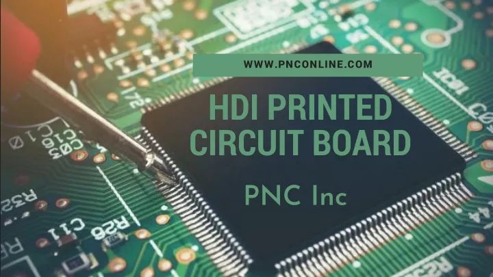
HDI stands for High Density Interconnect. HDI PCBs have finer traces and trace spacing, laser drilled micro vias and higher connection pad density. Its two chief advantages are that it permits the use of fine pitch BGAs and it reduces the number of PCB layers required because the finer traces and smaller vias allow more circuitry in a smaller area.

E N D
WWW.PNCONLINE.COM HDI PRINTED CIRCUIT BOARD PNC Inc
WHAT IS HDI PRINTED CIRCUIT BOARD • HDI stands for High Density Interconnect. HDI PCBs have finer traces and trace spacing, laser drilled micro vias and higher connection pad density. Its two chief advantages are that it permits the use of fine pitch BGAs and it reduces the number of PCB layers required because the finer traces and smaller vias allow more circuitry in a smaller area.
NARROW TRACE WIDTHS MEAN HIGHER CIRCUIT DENSITY • At PNC standard PC Board fabrication uses a minimum trace width of 5 mil, with a 5 mil space between traces (5/5mil) PNC’s HDI trace widths can be as narrow as 3 mil with 3 mil spacing. • These finer traces allow 160% more traces in the same real estate. 3/3mil spacing will also allow two traces to escape between pads of a standard BGA, meaning less PCB layers are needed to fan out the pins from the BGA.
MICROVIAS ARE THE ENABLING TECHNOLOGY FOR HDI • Narrow trace widths used in HDI PC Board are a result of the gradual refinement of photolithography and etching technology. Microvias on the other hand, are a revolutionary innovation driven by the development of high powered lasers that can be controlled accurately enough to ablate a 3 mil hole through the surface layer of copper and underlying laminate, without damaging the underlying layer of copper. • The Printed Circuit Board designat PNC take advantage of this by locating the power and ground layers at the top of the stack up. Since all active components access power and ground, sometimes through multiple pins, having the power and ground layers directly below the component layer allows all those connections to be made directly by microvias. This leaves the component layers and layers beneath the power and ground layers completely unobstructed for signal routing. This has the added advantage of reducing parasitic capacitance because it eliminates the circuit stubs caused by plated through holes.
Two sided boards are typically fabricated with a combination of through holes and microvias. Though holes can be drilled just through the core, connecting the stacks on the top and bottom of the board from the lowest layer, or through holes can be drilled through the entire stack directly connecting the traces on the top and bottom component layers. • HDI PCBs are a necessity when using fine pitched BGAs, but they can also reduce cost on PCBs without fine pitched BGAs because of the reduced layer count. On your next PCB design services, talk to the experts at PNC. They can help you determine if HDI technology is can reduce your PCB cost by reducing layer count and shrinking the PCB size.
GET IN TOUCH • ADDRESS • 115 East Centre St. Nutley, NJ, 07110 • PHONE • (973) 284-1600 • EMAIL • sales@pnconline.com • WEBSITE • www.pnconline.com