Download
1 / 8
80 likes | 225 Views
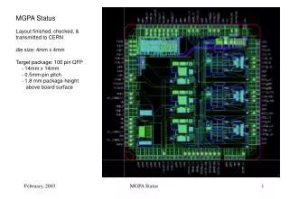
MGPA version 2 submission status – Mark Raymond / Jamie Crooks (RAL) 3 changes already proposed: 1) on-chip current reference present VFE card uses external circuit simple resistor to VDD -> supply voltage dependence 2) re-arrange digital signals to help VFE board layout

E N D
MGPA version 2 submission status – Mark Raymond / Jamie Crooks (RAL) 3 changes already proposed: 1) on-chip current reference present VFE card uses external circuit simple resistor to VDD -> supply voltage dependence 2) re-arrange digital signals to help VFE board layout allow routing of CALIN line away from chip inputs 3) Change I2C default settings set gain channel pedestals set CAL mode to ON and non-zero DAC setting 1 additional change: use spare pads either side of present QIN pad to triplicate QIN line reduces effective input inductance -> increased stability margin trivial layout change, worth having Ecal Electronics
measured pedestal dependence on supply voltage on-chip current reference improves pedestal stability to supply drift ~ 7.5 mV VDD drift -> 1 lsb pedestal drift (if Iref const.) (factor ~ 6 improvement on resistor to VDD) => worth having Ecal Electronics
on-chip current reference standard circuit (used before) Iref depends on Vth and R => process (but not supply) dependent put circuit in corner of chip near BIAS_IIN pad scrap BIAS_ENB function (not used) and replace by BIAS_IOUT (link on PCB) Vth R BIAS_IOUT BIAS_ENB BIAS_IIN BIAS_IIN VDD VDD VDD VDD 79 78 77 76 79 78 77 76 75 75 Ecal Electronics
re-arrange digital signals allows CALIN (2.5V transition) to route well away from MGPA I/P on VFE card (1 line for all 5 chips) => V1 and V2 pinouts not compatible TEST_MODE SDA_OUT TEST_DS RESET_N TEST_SO TEST_SI GND SCL VDD 100 99 98 97 96 95 94 93 92 SDA_OUT RESET_N TEST_DS TEST_SO TEST_SI CALIN CALIN 1 GND SCL VDD ADD0 OLD (V1) 2 100 99 98 97 96 95 94 93 92 ADD1 3 TEST_MODE 1 ADD0 NEW (V2) 2 ADD1 3 Ecal Electronics
change I2C default settings user request for non-zero default settings for pedestals, cal mode ON and non-zero DAC value chip usable (and testable) wthout I2C control problem: I2C block synthesized -> don’t want to re-synthesize and re-route (risk, time) solution: can make manual changes to wiring but each bit requires several cuts/straps X 3 (triplicated registers) => can be done but bigger job if several bits/register => limit changes to one bit/register all 3 pedestal registers default to 64 control register defaults to cal ON DAC defaults to 4 ( ~ 2/3 fullscale signal on high gain range for Cinj = 10 pF) NOTE: process/fabrication variations => optimum pedestal setting will still require I2C Ecal Electronics
Lin = 0 Lin = 8 nH 1st stage stability need series resistors to damp effect of parasitic L (bondwire/package) -> effective fix for current VFE card observed behaviour can be simulated – gain peaking in AC simulation -> instability in transient simulation stable if series resistor inserted Lin RS gain peaking AC simulation transient RS = 0 gain [Vout/Iin] RS = 10W frequency time Ecal Electronics
Lin = 0 Lin = 8 nH Leff = Lin/3 1st stage stability – any improvement possible? yes – if make use of spare pads either side of current Qin pad can reduce Lin by factor 3 minor change to wiring, no change to 1st stage layout -> improved stability margin -> worth having nc QIN 22 22 QIN QIN 23 23 nc QIN 24 24 AC and transient simulations for triplicated input pads BIAS2 BIAS2 25 25 26 27 26 27 Ecal Electronics
MGPA version 2 submission status summary 1) on-chip current reference 2) re-arrange digital signals to help VFE board layout 3) Change I2C default settings 4) modify QIN to 3 pads instead of 1 all layout changes completed and full DRC passed most of simulations complete some additional routine checks still outstanding (nothing major - won’t go into details here) estimated time required ~ only day or two more design transmission to CERN expected at end of this week (Friday 14th November) Ecal Electronics