Download
1 / 31
310 likes | 458 Views
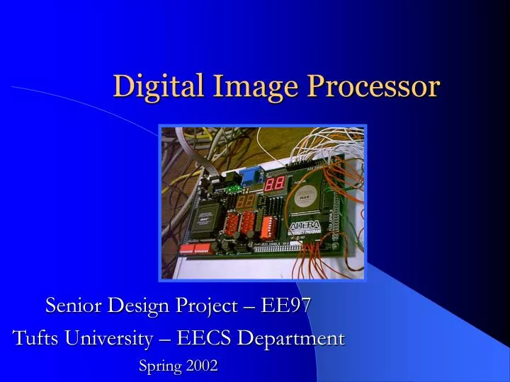
Digital Image Processor. Senior Design Project – EE97 Tufts University – EECS Department Spring 2002. Designed and Implemented by:. Paul D’Orlando - Computer Engineering ‘02 Weyant Stone - Computer Engineering ‘02 Yuri Grinshteyn - Computer Engineering ‘02.

E N D
Digital Image Processor Senior Design Project – EE97 Tufts University – EECS Department Spring 2002
Designed and Implemented by: • Paul D’Orlando - Computer Engineering ‘02 • Weyant Stone - Computer Engineering ‘02 • Yuri Grinshteyn - Computer Engineering ‘02
What is the Digital Image Processor? - Hardware component to perform outboard information processing - Memory interfaced with controller device - Ability to display input and output with built-in VGA interface
Four Major Questions 1. Where is the original image stored? 2. What moves and manipulates the image? 3. Where is the modified image stored? 4. How are the two images viewed?
Where is the Original Image Stored? - Read-only memory - Ability to store reasonably large amount of data - Non-volatile - Ease of programmability
What is an EPROM? - Eraseable Programmable Read-Only Memory - Non-volatile memory - Byte-addressable
The Am27C512 - 512K x 8 bit = 64Kbyte capacity - MegaMax downloader compatible - Asynchronous-access capable
What Moves and Manipulates the Image? - Controller logic - Requires easy programmability, fast prototyping, ease of testability - Common availability
Field-Programmable Gate Arrays (FPGA) - Industry standard for rapid prototyping - Programmable CMOS logic - Versatility vs. ASIC
The FLEX 10K20 - 20,000 gates - 189 user I/O pins - 3.3 – 5 volt operating range - ~13K RAM capacity - Built-in component of UP-1 board - Financially sensible
How are FPGAs Programmed? - Existing design (Verilog, VHDL, schematic) downloaded from PC via JTAG pins - Parallel port connection
Altera Max+PLUS II v10.1 - Compatibility with Flex10K20 chip - Support for code design - Familiarity - Financial sensibility
What are VHDL and Verilog? - Hardware description languages - Logic design using software algorithms - Easy specification of complex designs - Final logic is determined by compiler
ENTITY adder IS PORT( a, b :STD_LOGIC_IN, c, s :STD_LOGIC_OUT;) END adder; ARCHITECTURE add OF adder IS s = a XOR b; c = a AND b; END add; module adder(a, b, s, c); input a, b; output s, c; assign {s,c} = a + b; endmodule VHDL vs. Verilog
How to Program the FLEX 10K20 - Creating project file using software - Compiling, creating floorplan, determining pin assignment - Downloading
Features of the UP-1 - Components - Built-in JTAG and VGA interfaces - User I/O enabled - 25.175 Mhz on-board clock
Where is the Modified Image Stored? - SRAM • Static Random Access Memory • Easily rewritable • Addressing scheme similar to chosen EPROM
The UT621024 - 1024K x 8 bit = 128 Kbyte capacity - Byte-addressable - 5 volt operating range - Asynchronous read/write - Common I/O pins - Active low control
How Are the Two Images Viewed? - VGA interface • Video driver loaded as part of FPGA logic • VGA D-Sub port on UP-1 board • Select switch to determine whether contents of ROM or RAM are displayed
What is VGA? - Video Graphics Adapter - PC video output standard - 640 x 480 pixel display - 60 Hz refresh rate - Driven by 5 signals
The VGA Driver - Five output signals • Horizontal and Vertical Sync • Red, Green, Blue - Row and Column Counters - Uses onboard clock - Outputs one pixel per clock cycle
DEMO Design in Altera
What Does the Digital Image Processor Do? - EPROM Data • Holds 8 bars of different colors - FPGA Processes • Reads in and manipulates data from AM27C512 • Outputs processed data to UT621024 • Drives VGA output
DEMO -VGA and board operation
Conclusions - Learned Technology, Design Process - Design Goals achieved - Future Research Directions • Processing algorithm • VGA interface • Alternate Storage Media • ASIC Implementation
Special Thanks To… - Professor C. Hwa Chang - Professor Karen Panetta - Professor Stephen Morrison - Professor Soha Hassoun - Warren Gagosian - Paul Olsen - John Bottari - David Scher