Download
1 / 23
230 likes | 506 Views
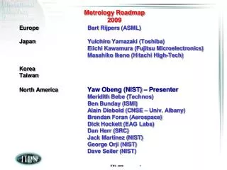
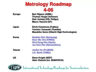
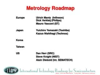
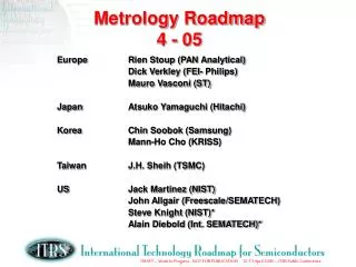
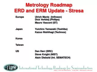
Metrology Roadmap. 2007. Metrology Roadmap 7-07 & 4-07. Europe Thomas Hingst (Qimonda) Bart Rijpers (ASML) Japan Masahiko Ikeno (Hitachi High-Technologies) Eiichi Kawamura (Fujitsu) Kazuhiro Honda (JEOL) Korea Taiwan North America John Allgair (AMD/ISMI)

E N D
Metrology Roadmap 2007 2007 ITRS DRAFT DO NOT PUBLISH
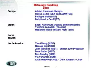
Metrology Roadmap7-07 & 4-07 Europe Thomas Hingst (Qimonda) Bart Rijpers (ASML) Japan Masahiko Ikeno (Hitachi High-Technologies) Eiichi Kawamura (Fujitsu) Kazuhiro Honda (JEOL) Korea Taiwan North America John Allgair (AMD/ISMI) Meredith Beebe (Technos) Ben Bunday (ISMI) Alain Diebold (CNSE – Univ. Albany) Dan Herr (SRC) Richard Hockett (CEA Labs) Mike Garner (Intel) Steve Knight (NIST) Jack Martinez (NIST) George Orji (NIST) Victor Vartanian (ISMI) 2007 ITRS DRAFT DO NOT PUBLISH
AGENDA • 2007 Changes • Lithography Metrology • FEP Metrology • Interconnect Metrology • ERM Metrology • Key Messages 2007 • Conclusions 2007 ITRS DRAFT DO NOT PUBLISH
2007 ITRS Changes 2007 ITRS DRAFT DO NOT PUBLISH
Replace Precision with Measurement Uncertainty 2007 ITRS DRAFT DO NOT PUBLISH
Overlay Metrology measurement uncertainty issue at 32 nm node (Double Patterning) 2007 ITRS DRAFT DO NOT PUBLISH
LER/LWR measurement • Test method is approved as a SEMI standard in Nov./2006 and • is available at SEMI homepage • P47-0307:“Test Method for Evaluation of Line-Edge Roughness and Linewidth Roughness” • Suggested measurement parameters are • Measurement length L : 2um or longer • Sampling interval ⊿y : 10nm or less • One of our collaboration results • among TWGs and related people Δy L 0.2 um Courtesy of A. Ymaguchi (Hitachi) 2007 ITRS DRAFT DO NOT PUBLISH
3D Metrology Requirements AA 2D grating top view example: • Recess Channel Device challenges: • complex grating-over-grating structure • includes overlay shift between the gratings • profile/geometry in different orientations is relevant • small profile features may berelevant (e.g. corner devices) 1 2 RC 3D grating 1 2 Deep Trench pattern (not present in test structures) 2007 ITRS DRAFT DO NOT PUBLISH
3D Metrology Requirements overlay shift creates asymmetry perfect overlay cross section example 2007 ITRS DRAFT DO NOT PUBLISH
FEP Metrology:Expanded Emphasis on Areas beyond High k • Increase in Mobility by using local stressing of transistors – FEPCall for local stress metrology in the channel • Metal Gates in production – Is routine Work Function measurement is a new requirement? • New transistor designs are advancing rapidly. Example: FIN-FETs require 3D metrology • Rapid annealing at 32/22 nm Generation will drive new dopant metrology needs & characterization of active carriers in transistors. 2007 ITRS DRAFT DO NOT PUBLISH
Cross sectioning Small laser spot for extracting single Tr. stress • Local Strain/Stress Measurement Proposal of new item on FEP table Relatively small laser spot (Visible light) with deeper penetration pMOS nMOS Ghani, et al (Intel) Wide laser spot for extracting average stress Measurement Point Stress Liner STI STI Channel Strain/Stress Modified from Fichtner’s figure 2007 ITRS DRAFT DO NOT PUBLISH
New table for Local Strain/Stress Measurementneed inputs from FEP and PIDS Table 120a Front End Processes Metrology Technology Requirements—Near-term Years Mobility Enhancement Factor For Idsat (Table 40ab) - Extended Planar Bulk - UTB FDS - DG Stress measurement with 50MPa resolution Spatial resolution (Offline, destructive, single Tr.) 1/5 of Gate Length Same size with HP Spatial resolution (Inline, non-destructive, Test pattern for average stress measurement) Using test pad of 100um X 100um Throughput (wafers/hour) (Inline, non-destructive, Test pattern) 25 sites per wafer 2007 ITRS DRAFT DO NOT PUBLISH
Local Strain/Stress Measurement Method (Tentative) Sensitivity Measurement Method Measurement Area Sample Thickness Area of Interest Stress Strain Transistor Level - CBED - NBD - TERS 20 MPa 100 MPa 50 MPa 0.02% 0.1% 0.05% 10-20nm ~10nm <50nm <100nm <300nm Destructive Destructive Destructive Non-Destructive Micro-Area Level 20 MPa 10 MPa 0.05% 0.01% ~150nm 100um - Confocal Raman - XRD - Photoreflectance Spectroscopy Non-Destructive Handling Area of ITRS Die - Die level flatness - Laser Interferometry - Coherent Gradient Sensing Non-Destructive Wafer - Laser Interferometry - Coherent Gradient Sensing 10 MPa 0.001% wafer Non-Destructive TERS (Tip Enhanced Raman Scattering) CBED (Convergent Beam Electron Diffraction) NBD (Nano Beam Electron Diffraction) XRD (X-ray Diffraction) * Stress – Strain relation : need to be clarified 2007 ITRS DRAFT DO NOT PUBLISH
Trend : Use Modeling to connect what you can measure with what you need to knowExample: Metrology of Strained Channel Devices MD Giles, et. al., VLSI Symposium 2004 2007 ITRS DRAFT DO NOT PUBLISH
Dopant profile measurement(Essentially destructive) • 2006 Update 10nm 10nm 10nm 1×10¹⁸atoms/cm3 Dan Herr - SRC Total throughput of analysis is one of remaining issues Do we need to put in a throughput requirement? 2007 ITRS DRAFT DO NOT PUBLISH
Wrap Around Gate FIN Wrap Around Gate Metrology Side Wall and Top Dielectric Thickness and Composition FINFET 2007 ITRS DRAFT DO NOT PUBLISH
Kreupl, Infineon • Carbon Nanotubes ? MARCO Center 2 mm Future Interconnect (ITRS 2007) • 3D Interconnect ? • Optical Interconnect ? Intel 2007 ITRS DRAFT DO NOT PUBLISH
2006/2007 Interconnect Activities • Air Gap based “dielectric” near term potential solution for 22 nm ½ pitch ≠porous low k • Air Gap sacrificial layer does not require unique metrology • Metrology is needed for 3D Integration • Alignment of chips for stacking – wafer level integration • Defects in bonding • Damage to metal layers • Defects in vias between wafers • Through Si via is high aspect ratio CD issue • Measurements of Sidewall barrier thickness and sidewall damage (compositional changes in low k) after etch remains a Major Gap - It will soon also be a Gap for FEP Metrology • New - Porous low k is projected for 32 nm ½ Pitch. 2007 ITRS DRAFT DO NOT PUBLISH
Metrology for Emerging Research Devices and Materials – 2007 ERM Teleconferences • Atomic and nanoscale structure (including defects) of low Z materials, such as carbon nanotubes and graphitic materials • Correlate nanostructure to macro-scale:bandgap, contact resistance, adhesion, mobility, dynamic properties, and nano-mechanical properties • Uniformity measurements of nanoscale properties over large areas • In-Situ measurements that enable enhanced synthetic and process control Aberration corrected HR-TEM of CNT with KI Metrology enables understanding the effect of crystal twins on mobility and mechanical properties 2007 ITRS DRAFT DO NOT PUBLISH
Metrology for Emerging Research Devices and Materials – 2007 ERM Teleconferences Dimensional Confinement effects Properties and metrology • Nondestructive 3D imaging of embedded interface, nanostructure, and atomic scale matrix properties • Optical properties of isolated and integrated low dimensional materials • Methods that resolve and separate surface from bulk • Integrated metrology and modeling tools that deconvolve probe - sample interactions • Nanoparticle monitors for ES&H, which include size, dose, and composition. Simulation shows ebeam skiping to next atomic column 2007 ITRS DRAFT DO NOT PUBLISH
Metrology Key Messages • Litho Metrology • Dual Patterning Overlay Metrology • Overlay Metrology Capability for Single Layer in RED for 45 nm ½ pitch • Overlay Definition for 32 nm ½ Pitch? • Tightened to 70% of single layer • Challenge of High Aspect Ratio Contact Hole Metrology • SEMI Standard for LER / LWR accepted • Wafer Sampling Methodology Section added • New Uncertainty Definition- replace Precision • Main challenge to CD Metrology before 32 nm ½ pitch is tool matching • 3D Dimensional and Shape Metrology for FEP, Interconnect and Litho 2007 ITRS DRAFT DO NOT PUBLISH
Metrology Key Messages • FEP Metrology • Stress/Strain Metrology Requirements added in 2007 • 2D/3D Dopant Profiling turn around time requirement added in 2007 • Interconnect Metrology • 3D Interconnect Metrology added in 2007 2007 ITRS DRAFT DO NOT PUBLISH
Conclusions • CD Measurement improvements show a path to the 32 nm Node • Propose definition for LWR and including LER • Transistor channel engineering requires Stress and Mobility Measurement • Interconnect requires Sidewall Measurements for barrier/seed and low trench • ERM and ERD require both improved imaging (such as aberration corrected TEM) and image simulation 2007 ITRS DRAFT DO NOT PUBLISH