Download
1 / 37
370 likes | 517 Views
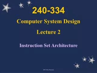
241-440 Computer System Design Lecture 4. Wannarat Suntiamorntut. Part I : Single Data Path. Outline. Design a Processor step by step Requirement of instruction set Components and clocking Testing Datapath Control Datapath. Processor. Datapath. M E M O R Y. Input. Control.

E N D
241-440Computer System DesignLecture 4 Wannarat Suntiamorntut 241-440 @ W.S.
Part I : Single Data Path 241-440 @ W.S.
Outline • Design a Processor step by step • Requirement of instruction set • Components and clocking • Testing Datapath • Control Datapath 241-440 @ W.S.
Processor Datapath M E M O R Y Input Control Output Five Component of Computer 241-440 @ W.S.
Performance Perspective • Performance of machine is determined by CPI • Processor Design : clock cycle time clock per instruction • Single cycle processor : adv. : one clock cycle per instruction disadv. : long cycle time 241-440 @ W.S.
Design Processor Step by Step 1. Analyze instruction set ==> Datapath requirement 2. Selection Set of datapath and establish clocking methodology 3. Assembly datapath meeting requirement 4. Analyze implementation of each instruction to determine setting of control 5. Assembly the control logic 241-440 @ W.S.
MIPS Instruction Format 241-440 @ W.S.
Step 1 • ADDU rd, rs, rt SUBU rd, rs, rt • ORI rt, rs, imm16 241-440 @ W.S.
Step 1 • lw rt, rs ,imm16 sw rt, rs, imm16 • beq rs, rt, imm16 241-440 @ W.S.
RTL • All instructions start by fetching Mem[PC] ADDU rd <= rs + rt; PC = PC + 4 SUBU rd <= rs + rt; PC = PC + 4 Ori rt <= rs + zero_ext(imm16);PC = PC + 4 LOAD rt <= mem[rs] + sign_ext(imm16); PC=PC + 4 STORE mem[rs] + sign_ext(imm16)<=rt; PC=PC+4 BEQ if rs = rt then PC=PC+sign_ext(imm16)||00 else PC = PC + 4 241-440 @ W.S.
Step 1 : The requirement from instruction • Memory Data & Instruction • Register (32 x 32) Read rs Read rt Write rt or rd • PC • Extender • Add and sub register or extend immediate • Add 4 or extended immediate to PC 241-440 @ W.S.
Step 2 : Components of datapath • Combination Element • Storage elements Clocking methodology 241-440 @ W.S.
Combination Elements Adder MUX 241-440 @ W.S.
Combination Elements ALU 241-440 @ W.S.
Storage Element : Register • Similar to D-flip/flop • Write enable negated(0) : Data out won’t change asserted(1) : Data out will be data in 241-440 @ W.S.
Register file • Consist of 32 registers • Ra select register to bus A • Rb select register to bus B • Rw select register to be written via bus W 241-440 @ W.S.
Storage : Ideal Memory • One Input • One Output • Memory word is selected by Address, Write enable = 1 then the data will be written • Clock input : is a factor only during write operation • During read operation : behaves on combination logic. 241-440 @ W.S.
Clock Methodology 241-440 @ W.S.
Step 3 : • Register Transfer Requirements --> Datapath Assembly • Instruction Fetch • Read Operands and Execute Operation 241-440 @ W.S.
Step 3 a : Instruction Fetch Unit Update PC : Sequence Code: PC <= PC + 4 Branch and Jump : PC <- something else 241-440 @ W.S.
Step 3b : Add & Sub 241-440 @ W.S.
Register-Register Timing 241-440 @ W.S.
Step 3c :Logical Operations with Immed. 241-440 @ W.S.
Step 3d: Load operations 241-440 @ W.S.
Step 3e : Store Operations 241-440 @ W.S.
Step 3f: Branch instruction beq rs, rt, imme16 • mem[pc] • equal <= rs = rt • if (con eq 0) then PC<=PC+4+(signExt(imm16)x4); else PC <= PC + 4; 241-440 @ W.S.
Datapath for Branch Operations 241-440 @ W.S.
Put it all together 241-440 @ W.S.
Abstract view of critical path 241-440 @ W.S.
Step 4 : Control Path 241-440 @ W.S.
Meaning of control signal • Rs, Rt and Imme16 hardwire to datapath • nPC_sel : 0 => PC • PC<= PC+4, 1 => PC • PC <= PC + 4 + signExt(Imm16) || 00 241-440 @ W.S.
Meaning of control signals ExtOp : Zero, sign MemWr:write memory ALUsrc: 0=>regB, 1=>imme Memtoreg:1=>mem ALUcrt : add, sub, or ReqWr : write dest. Reg. 241-440 @ W.S.
Control Signals 241-440 @ W.S.
Step 5 : Logic for each control signal 241-440 @ W.S.
Example : Load Flow 241-440 @ W.S.
Abstract View of implementation 241-440 @ W.S.
Next on Lecture 5 241-440 @ W.S.