Download
1 / 28
280 likes | 408 Views
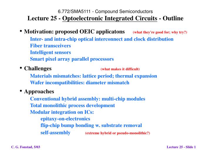
6.772/SMA5111 - Compound Semiconductors Lecture 25 - Optoelectronic Integrated Circuits - Outline. • Motivation: proposed OEIC applicatons (what they're good for; why try?) Inter- and intra-chip optical interconnect and clock distribution Fiber transceivers Intelligent sensors

E N D
6.772/SMA5111 - Compound SemiconductorsLecture 25 - Optoelectronic Integrated Circuits - Outline • Motivation: proposed OEIC applicatons(what they're good for; why try?) Inter- and intra-chip optical interconnect and clock distribution Fiber transceivers Intelligent sensors Smart pixel array parallel processors • Challenges(what makes it difficult) Materials mismatches: lattice period; thermal expansion Wafer incompatibilities: diameter mismatch • Approaches Conventional hybrid assembly: multi-chip modules Total monolithic process development Modular integration on ICs: epitaxy-on-electronics flip-chip bump bonding w. substrate removal self-assembly(extreme hybrid or pseudo-monolithic?) C. G. Fonstad, 5/03 Lecture 25 - Slide 1
Optical Solder Bumps: IC chip mountedmulti-chip module substrate C. G. Fonstad, 5/03 Lecture 25 - Slide 2
OEIC Applications: Smart Pixel Arrays“computation, parallel processing of data and images, en/decryption” C. G. Fonstad, 5/03 Lecture 25 - Slide 3
OEIC Applications: Diffuse optical tomography“seeing beneath the skin: tumors, blood vessels, bones, etc.” C. G. Fonstad, 5/03 Lecture 25 - Slide 4
Understanding the Significance of the Difference inthe Thermal Expansion Coefficients of Si and GaAs • Wafers of Si and GaAs with identical diameters of 150 mm* (6 in) at 15˚C: • If the temperature is raised 100˚C..... • ....the GaAs wafer becomes 70μm larger than the Si wafer! • • If the wafers are bonded, the stress is destructively large (i.e. they break) • • If the wafers are not bonded, any patterns on them are badly misaligned. - and - • A change of 100˚C is small; 500˚C or greater is more typical • * The industrial norm for Si is 200 mm (8 in), with 300 mm (12 in) diameter wafers becoming more common. C. G. Fonstad, 5/03 Lecture 25 - Slide 5
The other mismatch: Wafer Diameter MismatchThe newest silicon processes are fabricated on 200 mm (8 in),and more likely 300 mm (12 in), diameter wafers: C. G. Fonstad, 5/03 Lecture 25 - Slide 6
• Flip-chip p-i-n diode astride polymer waveguide/mirror Waveguide cross-section: 10 by 10 μm Die size: 750 μm square by 250 μm thick Optoelectronic integration - solder ball flip-chipassembly on opto-multi-chip module C. G. Fonstad,5/03 Lecture 25 - Slide 7
• Lasers or detectors flip-chip mounted on silicon chips with v-grooves etched to align to optical fibers (concept drawings) Note: V-grooves are formed using anisotropic etchants that reveal <111> planes (Images deleted) See FIgs. 12.12 and 12.13 in H.P. Zappe, Introduction to Semiconductor Integrated Optics. Artech House, Norwood, MA, 1995. Perspective Before: After: End view Concept drawings. Assemblies like this have been demonstrated. Optoelectronic integration - solder ball flip-chipassembly on a silicon chip The pulling and wetting action of the molten solder is strong enough to align the chips to the under-lying electronics. C. G. Fonstad, 5/03 Lecture 25 - Slide 8
(Images deleted) See Chapter 5 in J. Trezza et al, Heterogeneous Optoectonics Integration, E. Towe, ed. SPIE Press, Bellingham, WA, 2000. • BAE Systems, Xanoptics: Above: Schematic of process sequence Right: Solder bump formation and alignment Lower left: Photomicrograph of solder bump array. Lower right: Cross-section of QWIP array integrated using indium solder bump bonding OEIC Processes - Indium bump bondingwith substrate removal C. G. Fonstad, 5/03 Lecture 25 - Slide 9
OEIC Processes - Bump bondingwith substrate removal U. of Colorado co-planar process Left: Full assembly process Above: Top view of IC before and after integration Below: VCSEL prior to bonding (left) and after integration (rt) • (Images deleted) • See Chapter 4 in C. Wilmsen et al, Heterogeneous Optoectonics • Integration, E. Towe, ed. SPIE Press, Bellingham, WA, 2000. C. G. Fonstad, 5/03 Lecture 25 - Slide 10
OEIC Processes - Bump bonding with substrateremoval, cont. • U. of Colorado top-bottom • process • Left: Full assembly process • Below: Top view of IC after • integration • (Images deleted) • See Chapter 4 in C. Wilmsen et al, Heterogeneous Optoectonics • Integration, E. Towe, ed. SPIE Press, Bellingham, WA, 2000. C. G. Fonstad, 5/03 Lecture 25 - Slide 11
OEIC Processes - Bump bonding with substrate removal, cont. • U. of Colorado top contact • process • Left: Full assembly process • Below: Top view of IC after • integration • (Images deleted) • See Chapter 4 in C. Wilmsen et al, Heterogeneous Optoectonics • Integration, E. Towe, ed. SPIE Press, Bellingham, WA, 2000. C. G. Fonstad, 5/03 Lecture 25 - Slide 12
OEIC Processes - Bump bonding with dual-useheterostructures and substrate microlenses • • UCSB • Right: Cross-section of full • assembly • Lower left: VCSELs and • detectors fabricated • from the same hetero- • structure • Lower right: Microlens • array on stubstrate • (Images deleted) • See FIgs. 4.20, 4.18, and 4.16 in Coldren, L.A and Corzine S.W, Diode Lasers • and Photonic Integrated Circuits. New York: Wiley Interscience, 1995. C. G. Fonstad, 5/03 Lecture 25 - Slide 13
OEIC Processes - Total monolithic process development • • 4 full monolithic examples: • pin-HBT: • msm-HFET: • pin-HFET: • WGPD-HFET: C. G. Fonstad, 5/03 Lecture 25 - Slide 14
MIT Heterostructure Materials and Devices GroupThe Optical Solder Bump Concept for Integrating GaAs- andInP-based Heterostructure Devices with Si-CMOS ICsProf. Clifton G. Fonstad, MIT • Features: Commercial foundry ICs and heterostructures • Modular and monolithic; wafer-scale, batch processing • Planar topology; compatible with solder bump packaging • Current effort: Integrate and characterize high-speed 1550 nm photo- • diodes on CMOS chips; evaluate optical clock distribution concepts. • Future work: Develop the ultimate optical solder bump technology, • Magnetically Assisted Statistical Assembly (MASA). MASA will • enable us to integrate anything with anything! C. G. Fonstad, 5/03 Lecture 25 - Slide 15
MIT Heterostructure Materials and Devices Group C. G. Fonstad, 5/03 Lecture 25 - Slide 16
MIT Heterostructure Materials and Devices GroupEpitaxy-on-Electronics (EoE) • Commercially processed GaAs electronics (circuitry custom-designed using standard layout and simulation tools; chips obtained through MOSIS) •Monolithic processing, high surface planarity, no excessive overcoating of optoelectronic devices •All processing compatible with full-wafer and batch processing (no lattice or thermal expansion coefficient mismatch) •Conventional growth and fabrication of optoelectronic devices (growth temperatures must be under 475˚C) C. G. Fonstad, 5/03 Lecture 25 - Slide 17
MIT Heterostructure Materials and Devices GroupAn EoE-integrated LED on OPTOCHIPFIBE Cross-section by Dr. K. Edinger and Prof. J. Melngailis, Laboratory for Ion Beam Research and Application, University of Maryland C. G. Fonstad, 5/03 Lecture 25 - Slide 18 Courtesy of Dr. Edinger and Prof. Melngailis. Used with permission. Photo by Prof. Melngailis, melng@eng.umd.edu. Specimen provided by Prof. Fonstad.
MIT Heterostructure Materials and Devices GroupAligned Pillar Bonding (APB) • Optoelectronic heterostructures can be grown under optimal conditions on optimum substrates; bonded to GaAs or SOS •All features of EoE process retained; 3-d and SOS options added •Near-room temperature bonding would enable integration of InP- based optoelectronics and silicon-based electronics C. G. Fonstad, 5/03 Lecture 25 - Slide 19
MIT Heterostructure Materials and Devices GroupLayout of MIT MARCO Interconnect Focus CenterCMOS optical clock distribution test chip- designed and laid out by Nigel Drego and Mike Mills (Prof. D. Boning) Comments Technology: 0.18 μm CMOS Chip size: 2.2 x 2.2 mm Key feature: Designed to add photodetectors by aligned pillar bonding (APB) Recesses: 17 p-i-n detectors: InGaAs/InP (MBE- grown by Prof. Yoon Soon Fatt at NTU in Singapore) C. G. Fonstad, 5/03 Lecture 25 - Slide 20 Courtesy of Nigel Drego and Mike Mills. Used with permission. Prof. Duane Bonnings students (SM Thesis)
MIT Heterostructure Materials and Devices GroupDielectric recess on CMOS chip-recess geometry on MIT MARCO IFC optical clock distribution test chip- PiN heterostructures grown by Prof. Yoon Soon Fatt, NTU, Singapore - Comments Recess size: 50 by 50 microns Pillar size: 40 by 40 microns Recess bottom/back contact: formed in metal 2 Upper pad/top contact: formed in metal 7 C. G. Fonstad, 5/03 Lecture 25 - Slide 21
MIT Heterostructure Materials and Devices GroupOptical clock distribution using picosecond pulses RM3 integration makes it possible to meet the sub-10 fF challenge! C. G. Fonstad, 5/03 Lecture 25 - Slide 22
MIT Heterostructure Materials and Devices GroupConcepts for applying RM3 Integration(Recess mounting with monolithic metallization)to intra- and inter-chip optical interconnect Chip-to-chip interconnect at 40 Gbps using SiGe or InP mini-IC mux’s/demux’s, multi-contact in-plane lasers and detectors, and C. G. Fonstad, 5/03flexible planar waveguide ribbon cablesLecture 25 - Slide 23
MIT Heterostructure Materials and Devices GroupNano-pill assembly on processed Si IC wafes C. G. Fonstad, 5/03 Lecture 25 - Slide 24
MIT Heterostructure Materials and Devices GroupIII-V Heterostructure Nanopills- a GaAs nanopill etched free of its substrate Dimensions: diameter = 45 μm; height = 5 μm C. G. Fonstad, 5/03 Lecture 25 - Slide 25
OEIC Processes - DNA-assisted self assembly • • Two implementations: • Right: DNA-assisted attachment to a • carrier substrate,with subsequent • transfer and bonding to final Si host. • Below: DNA-assisted attachment to • host Si substrate directly • (Images deleted) • See p. 113-140 in Sadik C. Esener, Daniel Hartmann, Michael J. Heller, and Jeffrey M. Cable, "DNA Assisted • Micro-Assembly: A Heterogeneous Integration Technology for Optoelectronics," in Heterogeneous Integration: • Systems on a Chip, Ed. Anis Husain and Mahmoud Fallahi, Critical Reviews of Optical Engineering, Vol. CR70, SPIE • Optical Engineering Press, Bellingham, WA, 1998. • • Lock-and-key DNA-like chemicals • are used to encourage nanopills to • attach themselves to the appropriate • sites on the substrate surface C. G. Fonstad, 5/03 Lecture 25 - Slide 26
OEIC Processes - Fluidic self assembly • • Assembly of trapezoidal • nanopills in matching recesses • (Images deleted) • See Joseph J. Talghader, Jay K. Tu, and Stephen Smith, "Integration of Fluidically Self-Assembled Optoelectronic • Devices Using a Si-Based Process," IEEE Photon. Tech. Lett. 7 (1995) 1321-1323. C. G. Fonstad, 5/03 Lecture 25 - Slide 27
MIT Heterostructure Materials and Devices GroupMagnetically Assisted Statistical Assembly •Heterostructures grown under the optimal conditions on the optimum substrates. Close-packed pattern makes efficient use of epitaxial material. •IC wafers can be any material: e.g. Si, SOI, GaAs, InP (even ceramic or plastic). • Symmetrical bilateral pills greatly simplify assembly. High symmetry, a large excess of pills, and magnetic retention insure 100% filling of wells. •All monolithic, batch processing features of EoE process retained; three-dimensional integration now possible (as in APB). C. G. Fonstad, 5/03 Lecture 25 - Slide 28