Download
1 / 81
1.41k likes | 2.5k Views
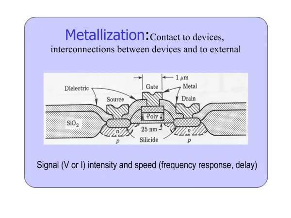
METALLIZATION. Objectives. Explain device application of metallization List three most commonly used metals List three different metallization methods Describe the sputtering process Explain the purpose of high vacuum in metal deposition processes. Types of Thin Film.

E N D
Objectives • Explain device application of metallization • List three most commonly used metals • List three different metallization methods • Describe the sputtering process • Explain the purpose of high vacuum in metal deposition processes
Types of Thin Film • Dielectric Film (CVD Process) • Oxide • Nitride • Epitaxial silicon • Conducting Film (PVD Process) • Aluminum alloy • Ti, TiN • Silicides • Copper (CVD or electroplating) • Tungsten (Metal CVD) • Polysilicon (LPCVD) Two Types of Thin Film
Metallization Metallization is an adding process that deposit metal layer on the wafer surface.
Requirements • Low resistivity for low power consumption and high IC speed. • High resistance to electromigration to achieve high chip reliability. • Low film stress for good adhesion to underlying substrate. • Stable mechanical and electrical properties during subsequent processing • Good corrosion resistance
Applications • Interconnection • Gate and electrodes • Micro-mirror • Fuse
CMOS: Std Metallization • Interconnection • Al-Cu alloy is commonly used material • Deep sub-micron metallization -Copper
Applications: Interconnection • Al dominate the metallization processes • Al-Cu alloy is most commonly used • W plug, technology of 80s and 90s • Ti, welding layer • TiN, barrier, adhesion and ARC layers • Now is Cu! • Future ???
Applications: Gate & Electrode • Al gate and electrode • Polysilicon replace Al as gate material • Silicide • – WSi2 • – TiSi2 • – CoSi2, MoSi2, TaSi2, … • Pt, Au, …as electrode for DRAM capacitors
Q & A Can we reduce all dimensions of metal interconnection line at the same ratio? When we shrink all dimensions (length l, width w, and height h) accordingly to the shrinking of the device feature size, resistance R increases, Slower circuit and more power consumption.
Conducting Thin Films • Polysilicon • Silicides • Aluminum alloy • Titanium • Titanium Nitride • Tungsten • Copper • Tantalum
Polysilicon • Gates and local interconnections • Replaced aluminum since mid-1970s • High temperature stability • Required for post implantation anneal process • Al gate can not use form self-aligned source/drain • Heavily doped • LPCVD in furnace
Silicide • Much lower resistivity than polysilicon • TiSi2, WSi2, and CoSi2 are commonly used
Silicide • TiSi2 and CoSi2 • Argon sputtering removes the native oxide • Ti or Co deposition • Annealing process forms silicide • Ti or Co don’t react with SiO2, silicide is formed at where silicon contacts with Ti or Co • Wet strips unreacted Ti or Co • Optional second anneal to increase conductivity
Tungsten Silicide • Thermal CVD process • – WF6 as the tungsten precursor • – SiH4 as the silicon precursor. • Polycide stack is etched • – Fluorine chemistry etches Wsix (Tungsten silicide) • – Chlorine chemistry etches polysilicon • Photoresist stripping • RTA increases grain size and conductivity
Aluminum • Most commonly used metal • The fourth best conducting metal • – Silver 1.6 mW°—cm • – Copper 1.7 mW°—cm • – Gold silver 2.2 mW°—cm • – Aluminum 2.65 mW°—cm • It was used for gate before mid-1970
Junction Spike • Al make direct contact with Si at source/drain • Si dissolves in Al and Al diffuses into Si • Junction spike • – Aluminum spikes punctuate doped junction • – Short source/drain with the substrate
Aluminum – Silicon Alloy • Prevent Junction Spike • ~1% of Si in Al saturates it • Thermal anneal at 400 °C to form Si-Al alloy at the silicon-aluminum interface
Electromigration • Aluminum is a polycrystalline material • Many mono-crystalline grains • Current flows through an aluminum line • Electrons constantly bombards the grains • Smaller grains will start to move • This effect is called electromigration
Electromigration • Electromigration tear the metal line apart • Higher current density in the remaining line • – Aggravates the electron bombardment • – Causes further aluminum grain migration • – Eventually will break of the metal line • Affect the IC chip reliability • Aluminum wires: fire hazard of old houses
Electromigration Prevention • When a small percent of copper is alloyed with aluminum, electromigration resistance of aluminum significantly improved • Copper serves as “glue” between the aluminum grains and prevent them from migrating due to the electron bombardment • Al-Si-Cu alloy was used • Al-Cu (0.5% - 4%\) is very commonly by the end 1990
Aluminum Alloy Deposition • PVD • – Sputtering • – Evaporation • Thermal • Electron beam • CVD • – Dimethylaluminum hydride [DMAH,Al(CH3)2H] • – Thermal process
Physical Vapor Deposition (PVD) Process • Physical Vapor Deposition • PVD works by vaporizing the solid materials, either by heating or by sputtering, and recondensing the vapor on the substrate to form the solid thin film. • Chemical Vapor Deposition • Gas(es) or vapor(s) chemically react on substrate surface and form solid by product on the surface as deposited thin film. • Other byproducts are gases and leave the surface. • Widely used in IC processing for metal, dielectric and silicon thin film deposition.
PVD vs. CVD • CVD: Chemical reaction on the surface • PVD: No chemical reaction on the surface • CVD: Better step coverage (50% to ~100%) and gap fill capability • PVD: Poor step coverage (~ 15%) and gap fill capability
PVD vs. CVD • PVD: higher quality, purer deposited film, higher conductivity, easy to deposit alloys • CVD: always has impurity in the film, lower conductivity, hard to deposit alloys
Titanium • Applications – Silicide formation – Titanium nitridation – Wetting layer – Welding layer
Application of Titanium • Reduce contact resistance. – Titanium scavenges oxygen atoms – Prevent forming high resistivity WO4 and Al2O3. • Use with TiN as diffusion barrier layer – Prevent tungsten from diffusing into substrate
Tungsten • Metal plug in contact and via holes contact holes become smaller and narrower • PVD Al alloy: bad step coverage and void • CVD W: excellent step coverage and gap fill • higher resistivity: 8.0 to 12 mW°—cm compare to PVD Al alloy (2.9 to 3.3 mW°—cm) • only used for local interconnections and plugs
Copper • Low resistivity (1.7 mW°—cm), • – lower power consumption and higher IC speed • High electromigration resistance • – better reliability • Poor adhesion with silicon dioxide • Highly diffusive, heavy metal contamination • Very hard to dry etch • – copper-halogen have very low volatility
Copper Deposition • PVD of seed layer • Electrochemical Plating (ECP) or CVD bulk layer • Thermal anneal after bulk copper deposition – increase the grain size – improving conductivity
Metal Thin Film Measurements • Thickness. • Stress • Reflectivity • Sheet resistance
Metal Thin Film Thickness • TEM and SEM • Profilometer • 4-point probe • XRF • Acoustic measurement
TEM and SEM • Cross section • TEM: very thin film, few hundred Å • SEM: film over thousand Å
Q & A ? Why is SEM photo is always in black and white? • Intensity of the secondary electron emission • – strong or weak signals • – photo image: bright and dim, black and white • SEM photo can be painted after it has been analyzed
Thickness Measurement • Metal films such as aluminum, Ti, TiN and copper are opaque films; therefore, optical-based technique such as reflectospectrometry cannot be used. • A destructive process is normally required to precisely measure the actual film thickness.
Profilometer • Thicker film (> 1000 Å), • Patterned etch process prior to measurement • Stylus probe senses and records microscopic surface profile
Acoustic Measurement • New technique • Directly measure opaque thin film thickness • Non-contact process, can be used for production wafer
Uniformity • The uniformity, in fact it is non-uniformity, of the thickness, sheet resistance, and reflectivity are routinely measured during the process development and for the process maintenance. • It can be calculated by measuring at multiple locations on a wafer
Mapping Patterns for UniformityMeasurement • Max-min uniformity (Max value – Min value) / (2 x average)
Uniformity • Most commonly used non-uniformity definition: 49-point, 3s standard deviation • Clearly define non-uniformity • For the same set of data, different definitions causes different results • 5-point and 9-point are commonly used in production
Stress • Stress is due to the mismatch between different materials • Compressive stress causes hillock, short between metal • Tensile stress causes crack, metal open, peel off • Two types of measurement • Contact – profilometer • Non-contact – capacitance measurement