Download
1 / 16
160 likes | 288 Views
Design of Pulsar Board. Mircea Bogdan (for Pulsar group) Level 2 Pulsar Mini-Review Wednesday, July 24, 2002. Level 2 Pulsar – Hardware Requirements. All the data interfaces that L2 decision crate has; Data source for all trigger inputs;

E N D
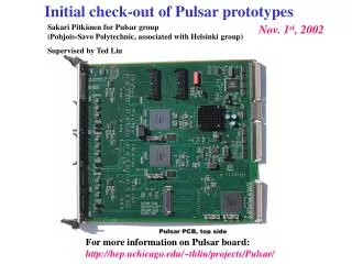
Design of Pulsar Board Mircea Bogdan (for Pulsar group) Level 2 Pulsar Mini-Review Wednesday, July 24, 2002
Level 2 Pulsar – Hardware Requirements • All the data interfaces that L2 decision crate has; • Data source for all trigger inputs; • Can record, reformat and retransmit data from upstream.
Level 2 Pulsar - Design Issues Parts: Factors considered: Price, existence of Synopsys simulation models, functionality; - FPGA for VME: EPM7128SOC160-7 - reuse from CDF Projects - $37. - FPGAs for Data I/O and Control: EP20K400BC652-1/2XV - $1,000/$560. uses +3.3V for I/O, +5V tolerant, hand assigned pins, we used ~10% of the logic elements for both the Data I/O and the Control chips; - FIFO 4Kx18 : CY7C4245-10ASC – reuse from SVT Projects - $8.40; - SRAM 128Kx36: CY7C1350-100AC - $40.45. POWER: -limited by the number of power pins on backplane; - uses +5V/ 13A (estimated); - generates: +2.5V/3A Max with LM1085IT-Adj.; - generates: +3.3V/15A Max with DATEL UNR-3.3/20 DC/DC; Over voltage Protection: 4-4.6Vcc. Big consumer: S-Link: Spec. Max. 6x4.5W/3.3V – Imax=8.18A. - will decide after prototype testing if we need to install DC/DC converter on the Aux card.
Level 2 Pulsar - Design Issues Configuration Options: - each FPGA has it’s own JTAG Chain with 3xEPC2LC20 and 10pin connector inside board; - one big chain with all 3xFPGAs and 9xEPC2s and 10 pin front panel connector. Clock Distribution: -CDF_CLK from P2 to each FPGA and each Mezzanine Card, used to latch L1A, L1 trigger data, etc. - 40 MHz S-LINK clock to each FPGA and to P3(optional) buffered with Robo Clock (skew programmed with jumpers), used to send S-LINK data – Oscillator on board. - 60 MHz algorithm clock to each FPGA used for algorithm, for SVT-FIFO read-out, for SRAM and mezzanine cards communications – Oscillator on board. - 53 MHz RF machine clock (optional) can replace the 60MHz clock, has 8pin AMP receptacle inside board with automatic on-board back-up with ICS581G-02: Zero Delay Glitch-Free Clock Mux.
Level 2 Pulsar – Mezzanine Cards • The board accepts 4 Mezzanine Cards, 2 for each Data I/O chip. • Each Mezzanine Card connected with Data(45:0) Bus and Ctrl(32:0) Bus that go directly to the FPGA; • Connections are bi-directional for flexibility; • CARD_ID(3:0) for identity check at power-up; prevents signal contention by keeping the I/Os in High Z; • Each MC is provided with +5V, +3.3V and +2.5V; • Design compatible with the Common Mezzanine Card Family Standard (CMC); • Two 64-pin surface-mount CMC connectors; Mezzanine Cards: - Hotlink I/O 4xCypressRx/Tx or 2xRx/Tx + lvds - prototype tested; - Taxi I/O 4x Taxi chips – not done yet; - ODIN S-LINK interface – commercially available 32-bit data with/40MHzCLK/160MBytes/s max transfer rate;
Level 2 Pulsar – Mezzanine Cards HotLinkRx HotLinkTx
Level 2 Pulsar - Trace Analysis We performed signal integrity test on some 80 nets on the board using the Interconnect Synthesis Tool by Mentor Graphics. Most of the IBIS models are vendor supplied. For the FPGAs we used QuartusII generated IBIS models. With NO Termination. With 33Ohm Series Termination on the Source.
Level 2 Pulsar - Functional Simulation • Each FPGA was first simulated with QuartusII 1.1. • Files imported in QuickSimII – Mentor Graphics • Extensive use of Synopsys SmartModels. • Connector-to-connector functional simulation of board. • Multi-board simulation: -instantiate Pulsar along with MCs in a top level schematic with DA; -run QSII with all the boards working together: 4xTx HotLink + 4xRx HotLink + Pulsar. • Possible: create a “virtual prototype” incorporating all the trace delays (SDF) generated with the trace analysis tool (ICX) into QSII.