Download
1 / 40
400 likes | 411 Views
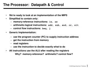
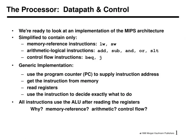
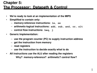
Processor: Datapath and Control. Single cycle processor Datapath and Control Multicycle processor Datapath and Control. Processor Design. Processor design datapath and control unit design processor design determines clock cycle time clock cycles per instruction

E N D
Processor: Datapath and Control • Single cycle processor • Datapath and Control • Multicycle processor • Datapath and Control
Processor Design • Processor design • datapath and control unit design • processor design determines • clock cycle time • clock cycles per instruction • Performance of a machine is determined by • Instruction count • clock cycle time • clock cycles per instruction
How to Design a Processor: step-by-step 1. Analyze instruction set => datapath requirements the meaning of each instruction is given by the register transfers datapath must include storage element for ISA registers possibly more datapath must support each register transfer 2. Select set of datapath components and establish clocking methodology 3. Assemble datapath meeting the requirements 4. Analyze implementation of each instruction to determine setting of control points that effects the register transfer. 5. Assemble the control logic
Single Cycle Processor • Single cycle processor • Pros: one clock cycle per instruction • Cons: too long cycle time, too low clocking frequency • Design a processor • analyze instruction set (the meaning of each instruction is given by the register transfers) • timing of each instruction • datapath support each register transfer • select datapath components and establish clocking methodology • analyze implementation of each instruction to determine setting of control points that affect register transfer • assemble control logic and datapath components
Clocking Methodology • Edge-triggered clock • setup time • hold time • all storage elements clocked by the same clock • combinational logic block: • inputs are updated at each clock tick • all outputs must be stable before the next clock tick
What is the smallest T that produces correct operation? Worst case CL delay limits T. Timing Analysis, Logic Delay
CLK == 0 Sense D, but Q outputs old value. CLK 0->1 Capture D, pass value to Q Flip Flop delays: clk-to-Q ? setup ? hold ? D Q CLK setup hold clk-to-Q
D Q Value of D is sampled on positive clock edge. t_setup CLK t_clk-to-Q Flip Flops have internal delays Q outputssampledvalue for rest of cycle. CLK D Q
Combinational Logic ALU “time budget”
31 26 21 16 11 6 0 op rs rt rd shamt funct 6 bits 5 bits 5 bits 5 bits 5 bits 6 bits 31 26 21 16 0 immediate op rs rt 6 bits 5 bits 5 bits 16 bits 31 26 0 op target address 6 bits 26 bits The MIPS Instruction Formats • All MIPS instructions are 32 bits long. The three instruction formats: • R-type • I-type • J-type • The different fields are: • op: operation of the instruction • rs, rt, rd: the source and destination register specifiers • shamt: shift amount • funct: selects the variant of the operation in the “op” field • address / immediate: address offset or immediate value • target address: target address of the jump instruction
Register Transfers • add $1, $2, $3; rs = $2, rt = $3, rd = $1 R[rd] <- R[rs] + R[rt} PC <- PC + 4 • sub $1, $2, $3; rs = $2, rt = $3, rd = $1 R[rd] <- R[rs] - R[rt] PC <- PC + 4 • ori $1, $2, 20; rs = $2, rt = $1 R[rt] <- R[rs] + zero_ext(imm16) PC <- PC + 4 • lw $1, 200($2); rs = $2, rt = $1 R[rt] <- MEM{R[rs] + sign_ext(imm16)} PC <- PC + 4 • sw $1, 200($2); rs = $2, rt = $1 MEM{R[rs] + sign_ext(imm16)} <- R[rt] PC <- PC + 4
Components Memory: hold instruction and data Registers: 32 32-bit registers • read rs • read rt • write rd • write rt Program counter Extender Add and Sub registers or extended immediates Add 4 to PC or Add extended immediate to PC (jump inst)
Combinational Logic Elements CarryIn (to add values) (to chose between values) (to do add, subtract, or) A 32 Sum Adder 32 B Carry • Adder • MUX(multi-plexor) • ALU 32 Select A 32 Y MUX 32 B 32 OP A 32 Result ALU 32 B 32
Storage Element: Register (Basic Building Block) • Register • Similar to the D Flip Flop except • N-bit input and output • Write Enable input • Write Enable: • negated (0): Data Out will not change • asserted (1): Data Out will become Data In Write Enable Data In Data Out N N Clk
Sequential Logic Elements • Registers: n-bit input and output, D F/F, write enable • rs, rt, rd : register specifiers read register1 read data1 read register2 write register write data read data2 registers
Fetching Instructions • Fetching instructions involves • reading the instruction from the Instruction Memory • updating the PC to hold the address of the next instruction Add 4 Instruction Memory Read Address PC Instruction • PC is updated every cycle, so it does not need an explicit write control signal • Instruction Memory is read every cycle, so it doesn’t need an explicit read control signal
Read Addr 1 Read Addr 1 Read Data 1 Read Data 1 Register File Register File Read Addr 2 Read Addr 2 Write Addr Write Addr Read Data 2 Read Data 2 Write Data Write Data Decoding Instructions • Decoding instructions involves • sending the fetched instruction’s opcode and function field bits to the control unit Control Unit Instruction • reading two values from the Register File • Register File addresses are contained in the instruction
31 25 20 15 10 5 0 R-type: op rs rt rd shamt funct Executing R Format Operations • R format operations (add, sub, slt, and, or) • perform the (op and funct) operation on values in rs and rt • store the result back into the Register File (into location rd) RegWrite ALU control Read Addr 1 Read Data 1 Register File Read Addr 2 overflow Instruction zero ALU Write Addr Read Data 2 Write Data • The Register File is not written every cycle (e.g. sw), so we need an explicit write control signal for the Register File
RegWrite ALU control MemWrite overflow zero Read Addr 1 Read Data 1 Address Register File Read Addr 2 Instruction Data Memory Read Data ALU Write Addr Read Data 2 Write Data Write Data MemRead Sign Extend 16 32 Executing Load and Store Operations • Load and store operations involves • compute memory address by adding the base register (read from the Register File during decode) to the 16-bit signed-extended offset field in the instruction • store value (read from the Register File during decode) written to the Data Memory • load value, read from the Data Memory, written to the Register File
Executing Branch Operations • Branch operations involves • compare the operands read from the Register File during decode for equality (zero ALU output) • compute the branch target address by adding the updated PC to the 16-bit signed-extended offset field in the instr Branch target address Add Add 4 Shift left 2 ALU control PC zero (to branch control logic) Read Addr 1 Read Data 1 Register File Read Addr 2 Instruction ALU Write Addr Read Data 2 Write Data Sign Extend 16 32
Executing Jump Operations • Jump operation involves • replace the lower 28 bits of the PC with the lower 26 bits of the fetched instruction shifted left by 2 bits Add 4 4 Jump address Instruction Memory Shift left 2 28 Read Address PC Instruction 26
Creating a Single Datapath from the Parts • Assemble the datapath segments and add control lines and multiplexors as needed • Single cycle design – fetch, decode and execute each instructions in one clock cycle • no datapath resource can be used more than once per instruction, so some must be duplicated (e.g., separate Instruction Memory and Data Memory, several adders) • multiplexors needed at the input of shared elements with control lines to do the selection • write signals to control writing to the Register File and Data Memory • Cycle time is determined by length of the longest path
Add RegWrite ALUSrc ALU control MemWrite MemtoReg 4 ovf zero Read Addr 1 Instruction Memory Read Data 1 Address Register File Read Addr 2 Data Memory Read Address PC Instruction Read Data ALU Write Addr Read Data 2 Write Data Write Data MemRead Sign Extend 16 32 Fetch, R, and Memory Access Portions
31 25 0 J-type: op target address Adding the Control • Selecting the operations to perform (ALU, Register File and Memory read/write) • Controlling the flow of data (multiplexor inputs) 31 25 20 15 10 5 0 R-type: op rs rt rd shamt funct 31 25 20 15 0 • Observations • op field always in bits 31-26 • addr of registers to be read are always specified by the rs field (bits 25-21) and rt field (bits 20-16); for lw and sw rs is the base register • addr. of register to be written is in one of two places – in rt (bits 20-16) for lw; in rd (bits 15-11) for R-type instructions • offset for beq, lw, and sw always in bits 15-0 I-Type: address offset op rs rt
Single Cycle Datapath with Control Unit 0 Add Add 1 4 Shift left 2 PCSrc ALUOp Branch MemRead Instr[31-26] Control Unit MemtoReg MemWrite ALUSrc RegWrite RegDst ovf Instr[25-21] Read Addr 1 Instruction Memory Read Data 1 Address Register File Instr[20-16] zero Read Addr 2 Data Memory Read Address PC Instr[31-0] 0 Read Data 1 ALU Write Addr Read Data 2 0 1 Write Data 0 Instr[15 -11] Write Data 1 Instr[15-0] Sign Extend ALU control 16 32 Instr[5-0]
R-type Instruction Data/Control Flow 0 Add Add 1 4 Shift left 2 PCSrc ALUOp Branch MemRead Instr[31-26] Control Unit MemtoReg MemWrite ALUSrc RegWrite RegDst ovf Instr[25-21] Read Addr 1 Instruction Memory Read Data 1 Address Register File Instr[20-16] zero Read Addr 2 Data Memory Read Address PC Instr[31-0] 0 Read Data 1 ALU Write Addr Read Data 2 0 1 Write Data 0 Instr[15 -11] Write Data 1 Instr[15-0] Sign Extend ALU control 16 32 Instr[5-0]
Load Word Instruction Data/Control Flow 0 Add Add 1 4 Shift left 2 PCSrc ALUOp Branch MemRead Instr[31-26] Control Unit MemtoReg MemWrite ALUSrc RegWrite RegDst ovf Instr[25-21] Read Addr 1 Instruction Memory Read Data 1 Address Register File Instr[20-16] zero Read Addr 2 Data Memory Read Address PC Instr[31-0] 0 Read Data 1 ALU Write Addr Read Data 2 0 1 Write Data 0 Instr[15 -11] Write Data 1 Instr[15-0] Sign Extend ALU control 16 32 Instr[5-0]
Load Word Instruction Data/Control Flow 0 Add Add 1 4 Shift left 2 PCSrc ALUOp Branch MemRead Instr[31-26] Control Unit MemtoReg MemWrite ALUSrc RegWrite RegDst ovf Instr[25-21] Read Addr 1 Instruction Memory Read Data 1 Address Register File Instr[20-16] zero Read Addr 2 Data Memory Read Address PC Instr[31-0] 0 Read Data 1 ALU Write Addr Read Data 2 0 1 Write Data 0 Instr[15 -11] Write Data 1 Instr[15-0] Sign Extend ALU control 16 32 Instr[5-0]
Branch Instruction Data/Control Flow 0 Add Add 1 4 Shift left 2 PCSrc ALUOp Branch MemRead Instr[31-26] Control Unit MemtoReg MemWrite ALUSrc RegWrite RegDst ovf Instr[25-21] Read Addr 1 Instruction Memory Read Data 1 Address Register File Instr[20-16] zero Read Addr 2 Data Memory Read Address PC Instr[31-0] 0 Read Data 1 ALU Write Addr Read Data 2 0 1 Write Data 0 Instr[15 -11] Write Data 1 Instr[15-0] Sign Extend ALU control 16 32 Instr[5-0]
Branch Instruction Data/Control Flow 0 Add Add 1 4 Shift left 2 PCSrc ALUOp Branch MemRead Instr[31-26] Control Unit MemtoReg MemWrite ALUSrc RegWrite RegDst ovf Instr[25-21] Read Addr 1 Instruction Memory Read Data 1 Address Register File Instr[20-16] zero Read Addr 2 Data Memory Read Address PC Instr[31-0] 0 Read Data 1 ALU Write Addr Read Data 2 0 1 Write Data 0 Instr[15 -11] Write Data 1 Instr[15-0] Sign Extend ALU control 16 32 Instr[5-0]
Adding the Jump Operation Instr[25-0] 1 Shift left 2 28 32 26 0 PC+4[31-28] 0 Add Add 1 4 Shift left 2 PCSrc Jump ALUOp Branch MemRead Instr[31-26] Control Unit MemtoReg MemWrite ALUSrc RegWrite RegDst ovf Instr[25-21] Read Addr 1 Instruction Memory Read Data 1 Address Register File Instr[20-16] zero Read Addr 2 Data Memory Read Address PC Instr[31-0] 0 Read Data 1 ALU Write Addr Read Data 2 0 1 Write Data 0 Instr[15 -11] Write Data 1 Instr[15-0] Sign Extend ALU control 16 32 Instr[5-0]
Single Cycle Control Unit: ALU control Instr[5-0] control unit Instr[31-26] ALU control to ALU operation ALUOp add sub. add sub. and or set on less than On page 302, Operation has 4 bits with the first bit always zero
On page 301, ALU control lines = Operation ALU control lines Function 0000 AND 0001 OR 0010 add 0110 subtract 0111 set on less than 1100 NOR