Download
1 / 19
230 likes | 470 Views
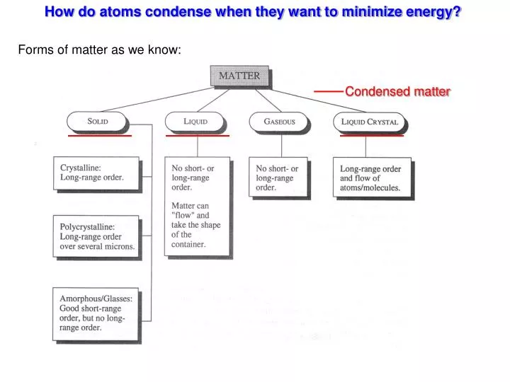
How do atoms condense when they want to minimize energy?. Forms of matter as we know:. Condensed matter. Crystal structures in materials. A unique arrangement of atoms that fill space in 3D (Real-life) when repeating (Translational Property).

E N D
How do atoms condense when they want to minimize energy? Forms of matter as we know: Condensed matter
Crystal structures in materials A unique arrangement of atoms that fill space in 3D (Real-life) when repeating (Translational Property) Everytime a unit cell is translated, it must be forming the entire lattice. 2D BCC 2D FCC
Is everything always in a crystalline order? Amorphization under electron bombardment in TEM
Short range order in 2D Extremely short range order Glassy silica (from wikipedia) Nematic liquid crystal (orientational long range order)
In 3D, there are seven types of crystal systems that make up 14 Bravais Lattices Triclinic, monoclinic, orthorhombic, tetragonal, rhombohedral, hexagonal and cubic X u1 X u3 r Translation vector = r T = r + u1a1 + u2 a2 + u3a3 X u2
The 14 Bravais lattices and their unit cell characteristics.
The Wigner-Seitz Cell can also be a unit cell Wigner-Seitz cell for sımple cubic in 3D Select a lattice point and draw construction lines to the nearest neighbouring points The smallest enclosed area represents the Wigner-Seitz cell. Here shown in orange. Draw lines that perpendicularly bisect the construction lines
No X interplanar distance We often deal with diffraction data of crystals. A real crystal can be expressed in reciprocal space (space-1) 1/a a b 1/b Unit cell in real space Unit cell in reciprocal space
Why deal with the reciprocal lattice? • Easy to deal with points rather than planes. • Every point represents a set of planes (a period that exists in your crystal). • Diffraction experiments yield the reciprocal lattice (It is the Fourier transform of a crystal – Believe it or not but nature takes the Fourier transform of your sample when carrying out, for instance, electron diffraction experiments in TEM or XRD). • Very useful when talking about electrons in a crystal (coming soon). Fourier Transform
Bragg’s equation: nλ = 2dsinθ Diffracted waves have to be in phase! (To see a “net reflected” wave)
A crystal can be thought of being a periodic function in a given space. What is meant by this? n(r+T) = n(r) Area of parallelogram Volume of the unit cell
z Primitive unit cells needed for the reciprocal primitive vectors FCC primitive cell y x BCC primitive cell
From International Union of CRYSTALLOGRAPHY (IUC) 2.1 Definition Let a, b, c be the basic vectors defining the unit cell of the direct lattice. The basic vectors of the reciprocal lattice are defined by: “The modulus of a* is equal to the ratio of the area of the face OBCG opposite to a to the volume of the cell built on the three vectors a, b, c. Referring to Figure below, we may write”:
TEM image and electron diffraction pattern from a piezoelectric thin film. How to guess any secondary formations in the structure that might detoriate or enhance your material? Structural interpretation of a high-k layer grown on Si. Note the dislocations at the interface that form as a result of ‘lattice misfit’.
An electron propagating in a crystal with wavelength a (k = 2π/λ) k Wave vector: Commonly used in discussing energies of electrons Larger the k, higher the energy of the electron (inverse of wavelength is quite convenient when representing energies) a: lattice constant