Download
1 / 2
20 likes | 155 Views
Melting of Silica-Embedded Ge Nanocrystals Eugene E. Haller, University of California, Berkeley, DMR-0405472.

E N D
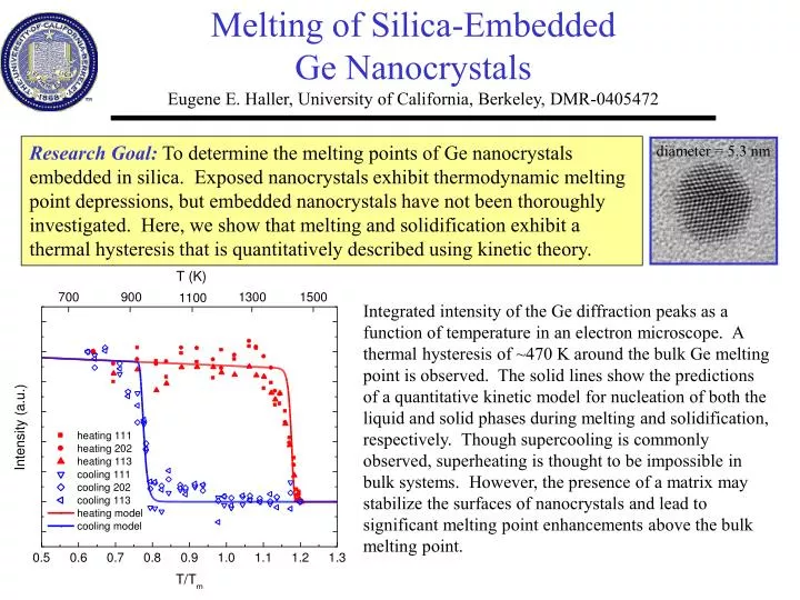
Melting of Silica-Embedded Ge NanocrystalsEugene E. Haller, University of California, Berkeley, DMR-0405472 Research Goal: To determine the melting points of Ge nanocrystals embedded in silica. Exposed nanocrystals exhibit thermodynamic melting point depressions, but embedded nanocrystals have not been thoroughly investigated. Here, we show that melting and solidification exhibit a thermal hysteresis that is quantitatively described using kinetic theory. diameter = 5.3 nm Integrated intensity of the Ge diffraction peaks as a function of temperature in an electron microscope. A thermal hysteresis of ~470 K around the bulk Ge melting point is observed. The solid lines show the predictions of a quantitative kinetic model for nucleation of both the liquid and solid phases during melting and solidification, respectively. Though supercooling is commonly observed, superheating is thought to be impossible in bulk systems. However, the presence of a matrix may stabilize the surfaces of nanocrystals and lead to significant melting point enhancements above the bulk melting point.
Melting of Silica-Embedded Ge Nanocrystals Eugene E. Haller, University of California, Berkeley, DMR-0405472 Education: Four graduate students (Chris Liao, Ian Sharp, Chun Wei Yuan, and Swanee Shin) have contributed to this project at the University of California at Berkeley. During the past year, two additional students (Drs. Diana Yi and Qing Xu) worked on this project and completed their PhDs. The melting experiments were performed by Q. Xu, who has learned to perform a variety of advanced Transmission Electron Microscopy (TEM) techniques. C. Liao, I. Sharp, and S. Shin have gained experience with the synthesis, processing, and characterization (both electronic and optical) of nanostructures. D. Yi and C.W. Yuan have developed comprehensive theoretical models of the implantation, nucleation, and growth of the nanocrystals and the effects of post-processing on nanocrystal properties. Broader Impact: The advancement of nanoscale science and technology is expected to have a great impact on a diverse range of fields. As dimensions shrink, new challenges in manipulation and measurement arise that must be overcome. A primary goal of this project is to develop characterization and processing techniques that will allow for continued miniaturization. Reference: “Large melting point hysteresis of Ge nanocrystals embedded in SiO2,” Q. Xu, I.D. Sharp, C.W. Yuan, D.O. Yi, C.Y. Liao, A.M. Glaeser, A.M. Minor, J.W. Beeman, M.C. Ridgway, P. Kluth, J.W. Ager III, D.C. Chrzan, and E.E. Haller, accepted for publication in Physical Review Letters (2006).