Download
1 / 19
730 likes | 2.56k Views
目錄. 何謂 LED GaN 半導體材料之物理意義 LED 結構以及該層相關分析 LED 上游之磊晶製程技術 總結 參考資料. 2. 何謂 LED. 發光二極體 (Light-Emitting Diode , LED )是一種能發光的半導體電子元件,透過三價與五價元素所組成的複合光源。 自從 1993 年日亞化學藍光之父中村修二開發出波長 450 nm 亮度 1000 mcd 氮化鎵藍光二極體,從此發光二極體更與人們生活緊密結合。例如 : 戶外看板、交通號誌、汽車煞車燈等。. 3. ( nm ). 4. GaN 半導體材料之分析. 間接能隙半導體.

E N D
目錄 • 何謂LED • GaN半導體材料之物理意義 • LED 結構以及該層相關分析 • LED上游之磊晶製程技術 • 總結 • 參考資料 2
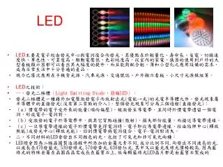
何謂LED • 發光二極體 (Light-Emitting Diode,LED)是一種能發光的半導體電子元件,透過三價與五價元素所組成的複合光源。 • 自從1993年日亞化學藍光之父中村修二開發出波長450 nm亮度1000 mcd氮化鎵藍光二極體,從此發光二極體更與人們生活緊密結合。例如:戶外看板、交通號誌、汽車煞車燈等。 3
(nm) 4
GaN半導體材料之分析 間接能隙半導體 直接能隙半導體 5
輻射複合 非輻射複合 6
LED 結構以及該層相關意義 p-contact 電流散佈層 ITO 提供電洞 Doping Mg p-GaN EBL電子阻擋層 Doping Mg p-AlGaN MQW 發光層 In0.25Ga0.75N/GaN n-GaN n-contact 提供電子 Doping Si n-GaN 緩衝層 buffer layer Sapphire 藍寶石基板 Chip size:300 x 300 μm2 7
Sapphire • 成分:Al2O3 • 厚度約300~400um(研磨後) • 升溫至1150 ℃-清除不必要的表面髒汙 Sapphire 8
Buffer Layer •成分:AlN或GaN •厚度約30nm •成長溫度約480~550℃ •容易跟Sapphire晶格匹配 buffer layer Sapphire 9
N-GaN •成分:GaN摻si •厚度約500nm~600nm •成長溫度約1050℃ •PN接面的N極 •提供電子(GaN五價+Si四價=9價,多一顆電子) Doping Si n-GaN buffer layer Sapphire 10
Multiple Quantum Well •成分:InGaN/GaN (well/barrier) •總厚度約50nm(看做幾對) •成長溫度約850℃ •使電子電洞更容易侷限在主動區增加複合機率 In0.25Ga0.75N/GaN Doping Si n-GaN buffer layer well barrier Sapphire 11
熱平衡下之 LED 能帶圖 偏壓下之 LED 能帶圖 12
Electron Blocking Layer •成分:p-AlGaN摻鎂 •成長溫度約950℃ •摻Al後位障會變高使電子較不會overflow Doping Mg p-AlGaN MQW Doping Si n-GaN buffer layer Sapphire 13
P-GaN •成分:GaN摻Mg •厚度約100nm~150nm •成長溫度約950~1120℃ •PN接面的P極 •提供電洞(GaN五價+Mg二價=7價,多一顆電洞) Doping Mg p-GaN Doping Mg p-AlGaN MQW Doping Si n-GaN buffer layer Sapphire 14
Indium Tin Oxide Transparent conductive layer •成分:氧化銦錫 •硬度高 •高電子傳導率 •低光吸收係數 •大面積鍍膜製程容易 •蝕刻製程容易 •受環境影響小 ITO Doping Mg p-GaN EBL MQW n-GaN Doping Si n-GaN buffer layer Sapphire 15
LED上游之磊晶技術 • 目前LED磊晶之機台都以(Metal Oxide Chemical Vapor Deposition)MOCVD為主,圖為相關原理。 16
參考資料 • 南台科大機械工程系http://elearning.stut.edu.tw/m_facture/Nanotech/Web/ch3.htm • 蝕刻技術http://elearning.stut.edu.tw/m_facture/ch9.htm • 晶元光電 • 臺灣師範大學機電科技學系-製程技術http://mems.ie.ntnu.edu.tw/document/class • 鍍膜技術http://me.csu.edu.tw/swl/non/ch8-2/ch8-2.pdf • 維基百科 20