Download
1 / 1
40 likes | 292 Views
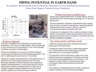
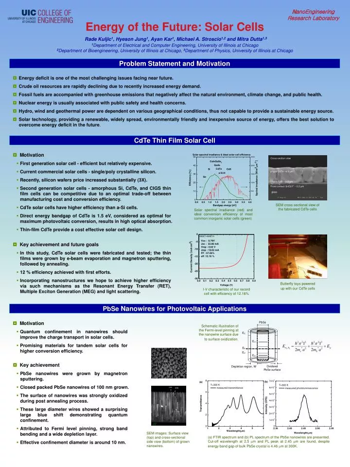
(111). 110 . Cross-section view. p-type CdTe ~4.5 μ m. n-type CdS ~ 0.2 μ m. Front contact SnO2:F ~ 0.2 μ m. glass. N anoEngineering Research Laboratory.

E N D
(111) 110 Cross-section view p-type CdTe ~4.5 μm n-type CdS ~ 0.2 μm Front contact SnO2:F ~ 0.2 μm glass NanoEngineering Research Laboratory Energy of the Future: Solar CellsRade Kuljic1, Hyeson Jung1, Ayan Kar1, Michael A. Stroscio1,2 and Mitra Dutta1,31Department of Electrical and Computer Engineering, University of Illinois at Chicago2Department of Bioengineering, University of Illinois at Chicago, 3Department of Physics, University of Illinois at Chicago Problem Statement and Motivation • Energy deficit is one of the most challenging issues facing near future. • Crude oil resources are rapidly declining due to recently increased energy demand. • Fossil fuels are accompanied with greenhouse emissions that negatively affect the natural environment, climate change, and public health. • Nuclear energy is usually associated with public safety and health concerns. • Hydro, wind and geothermal power are dependent on various geographical conditions, thus not capable to provide a sustainable energy source. • Solar technology, providing a renewable, widely spread, environmentally friendly and inexpensive source of energy, offers the best solution to overcome energy deficit in the future. CdTe Thin Film Solar Cell • Motivation • First generation solar cell - efficient but relatively expensive. • Current commercial solar cells - single/poly crystalline silicon. • Recently, silicon wafers price increased substantially (3X). • Second generation solar cells - amorphous Si, CdTe, and CIGS thin film cells can be competitive due to an optimal trade-off between manufacturing cost and conversion efficiency. • CdTe solar cells have higher efficiency than a-Si cells. • Direct energy bandgap of CdTe is 1.5 eV, considered as optimal for maximum photovoltaic conversion, results in high optical absorption. • Thin-film CdTe provide a cost effective solar cell design. SEM cross sectional view of the fabricated CdTe cells Solar spectral irradiance (red) and ideal conversion efficiency of most common inorganic solar cells (green) • Key achievement and future goals • In this study, CdTe solar cells were fabricated and tested; the thin films were grown by e-beam evaporation and magnetron sputtering, followed by annealing. • 12 % efficiency achieved with first efforts. • Incorporating nanostructures we hope to achieve higher efficiency via such mechanisms as the Resonant Energy Transfer (RET), Multiple Exciton Generation (MEG) and light scattering. Butterfly toys powered up with our CdTe cells I-V characteristic of our record cell with efficiency of 12.16% PbSe Nanowires for Photovoltaic Applications • Motivation • Quantum confinement in nanowires should improve the charge transport in solar cells. • Promising materials for tandem solar cells for higher conversion efficiency. Schematic illustration of the Fermi-level pinning at the nanowire surface due to surface oxidization. • Key achievement • PbSe nanowires were grown by magnetron sputtering. • Closed packed PbSe nanowires of 100 nm grown. • The surface of nanowires was strongly oxidized during post annealing process. • These large diameter wires showed a surprising large blue shift demonstrating quantum confinement. • Attributed to Fermi level pinning, strong band bending and a wide depletion layer. • Effective confinement diameter is around 10 nm. SEM images: Surface view (top) and cross-sectional side view (bottom) of grown nanowires. (a) FTIR spectrum and (b) PL spectrum of the PbSe nanowires are presented. Cut-off wavelength at 2.5 m and PL peak at 2.45 m are found, despite energy band gap of bulk PbSe crystal is 4.46 m at 300K.