Download
1 / 16
160 likes | 292 Views
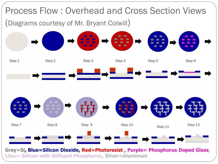
Process Flow : Overhead and Cross Section Views ( Diagrams courtesy of Mr. Bryant Colwill ). Step 1. Step 2. Step 3. Step 4. Step 5. Step 6. Step 7. Step 8. Step 9. Step 10. Step 12. Step 11. T. T. T. T. T. T. T. T. T. T. T. T. T. T. T. T. T. T. T. T. T. T. T.

E N D
Process Flow : Overhead and Cross Section Views (Diagrams courtesy of Mr. Bryant Colwill) Step 1 Step 2 Step 3 Step 4 Step 5 Step 6 Step 7 Step 8 Step 9 Step 10 Step 12 Step 11 T T T T T T T T T T T T T T T T T T T T T T T T T T T T T T T T T T T T T T T T Grey=Si, Blue=Silicon Dioxide, Red=Photoresist , Purple= Phosphorus Doped Glass, Lilac= Silicon with Diffused Phosphorus, Silver=Aluminum
Step 1: Cleaning Overhead View of Wafer First, we started with a positively charged, P-type, silicon wafer. We cleaned it with a mixture of sulfuric acid and hydrogen dioxide to remove surface impurities and reduce errors. Starting Si Wafer & Sulfuric Acid / Peroxide Clean Cross-section View of Wafer Si Wafer Color Code: Grey=Si, Blue=Silicon Dioxide, Red=Photoresist
Step 2: Deposition of Overhead View of Wafer The PECVD (Plasma Enhanced Vapor Deposition) Machine was used to heat the wafer to 400 degrees and react ionized gas with the wafer’s surface to add a film of silicon dioxide. Plasma Enhanced Chemical Vapor Deposition Of Silicon Dioxide Cross-section View of Wafer PECVD Machine Color Code: Grey=Si, Blue=Silicon Dioxide, Red=Photoresist
Step 3: Lithography Patterning Overhead View of Wafer Lithography comes from the Latin roots “lithos” and “graphy” meaning “writing on stone.” We used photolithography which involved using photosensitive chemicals and UV light to pattern the wafer. Lithography Patterning Cross-section View of Wafer Photolithography Machine Color Code: Grey=Si, Blue=Silicon Dioxide, Red=Photoresist
Step 3: Lithography Patterning (cont.) Overhead View of Wafer First, we applied HMDS to help adhere the photoresist, a photosensitive chemical. We then used spin coating at 4000 RPM to cover the surface of the wafer with a thin layer of photoresist. Next, we baked the covered wafer on a hot plate for a minute to harden the photoresist. The Spin Coater Lithography Patterning Cross-section View of Wafer Color Code: Grey=Si, Blue=Silicon Dioxide, Red=Photoresist
Step 3: Lithography Patterning (cont.) Overhead View of Wafer We covered the wafer with a mask that left some area exposed and protected others. Then, the wafer was exposed to UV light, which broke the cross-linked polymer chains in the uncovered photoresist. Next, we rinsed off the weakened photoresist with a weak base and then a water bath with bubbling nitrogen. This left the surface of the wafer patterned. UV Contact Aligner Machine Lithography Patterning Cross-section View of Wafer The Rinsing Station Color Code: Grey=Si, Blue=Silicon Dioxide, Red=Photoresist
Step 4: Acid Wash Overhead View of Wafer We used hydrogen fluoric acid to remove the exposed silicon dioxide layer. This revealed the base silicon of the wafer in regions not protected by cross-linked photoresist. Acid Washing Cross-section View of Wafer Acid Etching and Rinse Station Color Code: Grey=Si, Blue=Silicon Dioxide, Red=Photoresist
Step 5: Removal of Photoresist Overhead View of Wafer The wafer was cleaned of the remaining photoresist and impurities with hydroxide and sulfuric acid. Next, it was washed in water and placed in a rack to be spun dry in nitrogen gas. Photoresist Removed Cross-section View of Wafer Grey=Si, Blue=Silicon Dioxide, Red=Photoresist , Purple= Phosphorus Doped Glass, Lilac= Silicon with Diffused Phosphorus, Silver=Aluminum
Step 6: Phosphorous Doping Overhead View of Wafer The tube furnace was used to heat the wafer to 1100 degrees Celsius and expose it to , which grew a layer of phosphorous-doped glass on the regions not covered by silicon dioxide. This was in order to create the N-type well of the P-N junction. Phosphorous Doping Cross-section View of Wafer The Tube Furnace Grey=Si, Blue=Silicon Dioxide, Red=Photoresist , Purple= Phosphorus Doped Glass, Lilac= Silicon with Diffused Phosphorus, Silver=Aluminum
Step 7: Phosphorous Diffusion Overhead View of Wafer The phosphorous glass was removed, leaving a layer of negatively doped silicon. This is an essential feature of the P-N Junction. Diffusion of Phosphorous Cross-section View of Wafer Grey=Si, Blue=Silicon Dioxide, Red=Photoresist , Purple= Phosphorus Doped Glass, Lilac= Silicon with Diffused Phosphorus, Silver=Aluminum
Step 8: Aluminum Deposition Overhead View of Wafer The wafer was attached to a larger carrier wafer and placed in the sputtering machine to be coated with aluminum. Aluminum Coating Cross-section View of Wafer Sputtering Machine Grey=Si, Blue=Silicon Dioxide, Red=Photoresist , Purple= Phosphorus Doped Glass, Lilac= Silicon with Diffused Phosphorus, Silver=Aluminum
Step 9: Photolithography Overhead View of Wafer Photolithography was used again to pattern the wafer. The mask had to be aligned precisely with the patterning already on the wafer. The wafer was developed, rinsed, and baked to imprint the design. The covered areas will become the conductive circuitry of the final product. In the end, only select areas of the aluminum remained covered with photoresist. Photolithography Patterning T T T T T Cross-section View of Wafer T T T T T Grey=Si, Blue=Silicon Dioxide, Red=Photoresist , Purple= Phosphorus Doped Glass, Lilac= Silicon with Diffused Phosphorus, Silver=Aluminum
Step 10: Wet Etching Overhead View of Wafer The wafer was submerged in a mixture of acetic acid, phosphoric acid, nitric acid, and water to remove all of the exposed aluminum. Aluminum Removal by Acid Etch T T T T T T T T Cross-section View of Wafer T T Rinse Tank Grey=Si, Blue=Silicon Dioxide, Red=Photoresist , Purple= Phosphorus Doped Glass, Lilac= Silicon with Diffused Phosphorus, Silver=Aluminum
Step 11: Photoresist Removal Overhead View of Wafer The wafer was placed in an organic solvent called NMP for 5 minutes to remove the remaining photoresist. Photoresist Removed T T T T T Cross-section View of Wafer T T T T T Grey=Si, Blue=Silicon Dioxide, Red=Photoresist , Purple= Phosphorus Doped Glass, Lilac= Silicon with Diffused Phosphorus, Silver=Aluminum
Step 12: Aluminum Deposition Overhead View of Wafer The silicon dioxide on the bottom of the wafer was removed using hydrofluoric acid. The wafer was again put into the sputtering machine, this time to coat the bottom of the wafer with aluminum. This allowed for conductivity and a low resistance. Bottom Coated with Aluminum T T T T T Cross-section View of Wafer T T T T T Grey=Si, Blue=Silicon Dioxide, Red=Photoresist , Purple= Phosphorus Doped Glass, Lilac= Silicon with Diffused Phosphorus, Silver=Aluminum
Works Cited • http://cnx.org/content/m25495/latest/