Download
1 / 17
190 likes | 568 Views
Grating-Coupled SPR for rapid, label-free, array-based sensing. 指導教授:林啟萬 研究生:蘇明啟 日期: 2004/06/30. outline. Basis of grating-coupled SPR Structure of GC-SPR and Schottky Junction An experiment of GC-SPR Array-based GC-SPR Conclusion Reference. How does grating-coupled SPR occur.

E N D
Grating-Coupled SPR for rapid, label-free, array-based sensing 指導教授:林啟萬 研究生:蘇明啟 日期:2004/06/30
outline • Basis of grating-coupled SPR • Structure of GC-SPR and Schottky Junction • An experiment of GC-SPR • Array-based GC-SPR • Conclusion • Reference
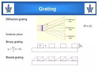
How does grating-coupled SPR occur The sensitivity of prism-coupled SPR sensor is a little higher than that of grating-based SPR sensor. However, GCSPR has advantages of small size, cheap, suitable for portable design.
The fabrication process of grating • I. • Start with fabrication by holographically with an blue laser (488 nm) on GaAs substrate with doping level from 5x10¹⁶ to 5x1018 cm-3 • The microstructure was revealed by AFM, which reconstructs the grating profile and determines groove depth and grating period. • Thermally evaporated metal (Au) films were deposited at room temperature. • II. • Exposing Shipley S1405-17 photoresist to two expanded collimated interfering beams of 457.9 nm radiation from an argon ion laser. • Hardened by exposure to ultra-violet radiation • Etched by an energetic atom beam to transfer the spatial profile in the photoresist through into the silica substrates.
Schottky Junction • 由金屬和N型半導體接合 • 接觸面上形成Schottky barrier • 加入順向偏壓時,N型區的自由電子獲得足夠能量,而移到較大的軌道中移動,因此自由電子也能跨越接面而進入金屬區,造成大量順向電流。 • 導通電壓低 • 極低雜訊指數
Band Diagram of a Metal-Semiconductor Junction Each material has a characteristic energy which is needed to remove an electron from its surface to infinity. This is called the work function of the material. When a high work function metal comes in contact with a semiconductor with a lower work function, electrons flow from the semiconductor to the metal. This results in a band configuration shown in Figure.
Schematic Diagram of GCSPR period d=652 nm height h~18 nm Incident angle of P-polarized light is 18˚
alcohol concentration vs angular shift • Alcohol concentration in water (%) • 0 • 7.3 • 13.6 • 19.2 • 24.0 • 28.3 incident angle vs short-circuit photocurrent
Make Use of Gratings on CD-ROM Plastic molded transducers (grating chips)
Grating-Coupled SPR Period is 867 nm Groove depth is 40 nm
Simultaneous Measurement on Microarrays avidin Biotin MUA+PL Au Film (80 nm) Plastic Grating MUA: 11-mercaptoundecanoic acid PL: electrostatically adsorbed Poly-L-lysine
SPR Curve: Incident angle vs Reflectance Principle of operating of kinetic analysis system. Light source: 867 nm LED SPR curves collected by CCD camera
Detection of Protein Binding Spot size 250 um 1-cm2 containing 400 spots
Reference • Jennifer M. Brockman, Salvador M. Fernandez, Grating-coupled surface plasmon resonance for rapid, label-free, array-based sensing, American Laboratory, June 2001 • N. L. Dmitruk, O. I. Mayeva, S. V. Mamykin, O. B. Yastrubchak, On a Control of Photo-surface Plasmon Coupling at a Multilayer Diffraction Grating, Institute for Physics of Semiconductors NAS of Ukraine, IEEE 2000 • Dmitruk N.L., Mayeva O.I., Mamykin S.V., Fursenko O.V., Yastrubchak O.B., Influence of Multilayer Coating Peculiarities on Efficiency of Surface Plasmon Resonance Photodetector, Institute of Physics of Semiconductors NAS of Ukraine, IEEE 1998 • R A Watts, J R Sambles, M C Hutley, T W Preist, C R Lawrence, A New Optical Technique for Characterizing Reference artefacts for Surface Profilometry, Thin Film Photonics Group, Department of Physics, University of Exeter, UK, National Physical Laboratory, Middlesex UK, Nanotechnology 8 (1997) 35-39 • http://www.formosams.com • http://nina.ecse.rpi.edu/shur/Ch3/sld043.htm • http://solarwww.mtk.nao.ac.jp/kobayash/thesis/node34.html