Download
1 / 19
190 likes | 314 Views
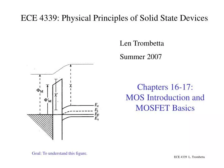
ECE 4339: Physical Principles of Solid State Devices. Len Trombetta Summer 2007. Chapters 16-17: MOS Introduction and MOSFET Basics. Goal: To understand this figure. The MOS capacitor (Fig. 16.1) contains most of the important physics of the MOS FET (Fig. 17.1).

E N D
ECE 4339: Physical Principles of Solid State Devices Len Trombetta Summer 2007 Chapters 16-17: MOS Introduction and MOSFET Basics Goal: To understand this figure. ECE 4339 L. Trombetta
The MOS capacitor (Fig. 16.1) contains most of the important physics of the MOS FET (Fig. 17.1). Basic MOSFET operation: with VG > VT, electrons (minority carriers) will collect at the interface between Si and SiO2 and create a connection between source and drain. If VD > VS, a current (ID) will flow. VD: drain voltage VS: source voltage VG: gate voltage VT: threshold (“turn-on”) voltage ECE 4339 L. Trombetta
In all these diagrams, the Fermi level is the solid line. It is always flat because we are in equilibrium. The dashed line is the intrinsic Fermi level. It follows the conduction and valence band edges so if there is band bending, the intrinsic Fermi level bends with them. We are assuming here that the Fermi level in the metal (on the left) is equal to the Fermi level in the semiconductor (on the right). If it is not, we have a minor complication, but the basic device physics is the same. ECE 4339 L. Trombetta
Charge in the metal is assumed to exist in a thin sheet near the oxide interface. Charge in the semiconductor will be distributed, as it is in a pn junction diode; we will also assume it is constant with distance. ECE 4339 L. Trombetta
Si-SiO2 interface In accumulation, majority carriers (electrons in this case) pile up at the Si-SiO2 interface. The Fermi level at the interface is very close to the conduction band edge, reflecting the build-up of electrons there. The Fermi level at the interface is near mid-gap (i.e., near Ei) so the number of both electrons and holes is small (depleted) compared with ND. The charge in the semiconductor is from ionized donors. Current does not flow, no matter what the sign of the bias; it cannot get past the large energy barriers presented by the insulator band gap. ECE 4339 L. Trombetta
The Fermi level at the interface is below Ei so the number of holes is larger than the number of electrons at the surface; we say the surface is inverted. The charge in the semiconductor is from ionized donors and now also includes the holes in the inversion layer. With increasing VG, the number of holes in the inversion layer increases. ECE 4339 L. Trombetta
qfs x = W Potential f is measured between the intrinsic Fermi level in the bulk and its value at some point in the depletion region. The value of the potential at the surface is fs, the surface potential. Note that fs is the voltage drop across the semiconductor. The depletion region extends from x = 0 to x = W. It is analogous to the depletion region on the p-type side of a pn junction diode. ECE 4339 L. Trombetta
qfF qfF 2qfF Onset of inversion This is the VG = VT case from Fig. 16-5 e above. It shows that the onset of inversion is defined as the point where the Fermi level at the surface is just as far below the intrinsic Fermi level as it is above it in the bulk. That means the total band bending is ECE 4339 L. Trombetta
The dark region between the source and drain represents the channel charge QN. The p-type body of the device contains ionized acceptors, which are “exposed” when the depletion region opens up (just as in a pn junction). The depletion region gets bigger toward the drain because a positive drain bias corresponds to reverse-bias of the pn junction formed by the drain and the p-type body. As the number of ionized acceptors increases, QN decreases above it. In (c), the reverse bias at the drain is large enough to completely deplete the channel charge there. This is the saturation point (ID does not increase further). ECE 4339 L. Trombetta
Mobility in the inversion layer is less than (typically ~ ½ ) the bulk mobility (the value you find in Table 3.5). This is because there is a new scattering mechanism: scattering from the interface. ECE 4339 L. Trombetta
The mobility of the carriers in the channel, m, and the number of carriers in the channel n, are complicated functions of position (both x and y). In modeling the current-voltage characteristics, we handle this by defining QN in terms of the capacitance of the gate oxide and the gate voltage, and by defining a surface mobility (which would need to be given). ECE 4339 L. Trombetta
This and the next slide are from Chapter 18. When the Fermi level in the metal and semiconductor are not equal, we get band bending at zero gate bias; this is analogous to the built-in potential in a diode. This introduces a shift in the threshold voltage equal to (EF,s – EF,m)/q. If FM and FS are expressed in volts, the shift is DVT = FM - FS. (The subscript “FB” refers to “flat bands”, which is the gate voltage necessary to get band bending to go to 0.) ECE 4339 L. Trombetta
Work function difference fMS = fM - fS (expressed in volts) for Al or n+ polysilicon gates. ECE 4339 L. Trombetta


![There Are No “Buts” in Progressive Enhancement [Øredev 2015]](https://cdn4.slideserve.com/7568391/slide1-dt.jpg)