Download
1 / 19
190 likes | 313 Views
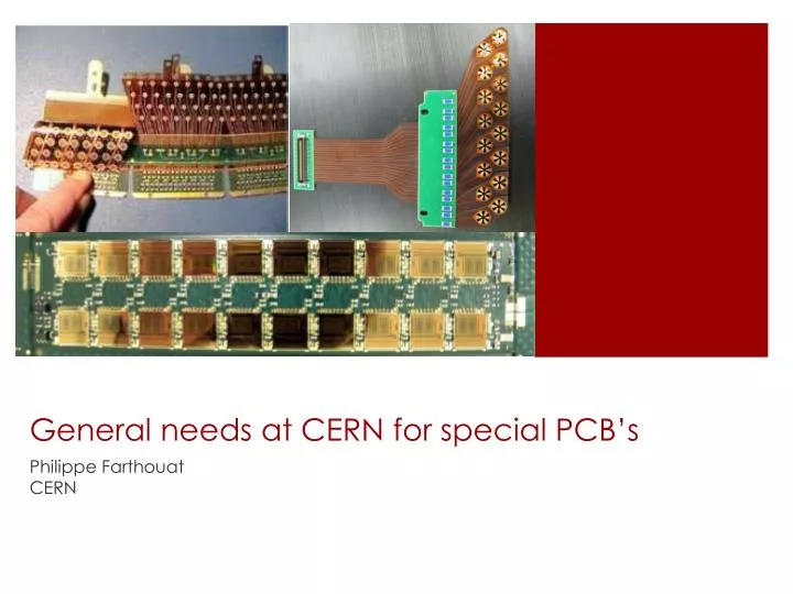
General needs at CERN for special PCB’s. Philippe Farthouat CERN. Outline. High density and low mass PCB’s for tracker front-end Rigid, flex and flex rigid Multilayer PCB’s for high speed applications Large size rigid and flex PCB’s for Micro-Pattern Gas Detectors (MPGD). Outline.

E N D
General needs at CERN for special PCB’s Philippe Farthouat CERN
Outline General Needs at CERN for special PCBs High density and low mass PCB’s for tracker front-end • Rigid, flex and flex rigid Multilayer PCB’s for high speed applications Large size rigid and flex PCB’s for Micro-Pattern Gas Detectors (MPGD)
Outline General Needs at CERN for special PCBs High density and low mass PCB’s for tracker front-end • Rigid, flex and flex rigid Multilayer PCB’s for high speed applications Large size rigid and flex PCB’s for Micro-Pattern Gas Detectors (MPGD)
High Density PCB’s for tracker front-end General Needs at CERN for special PCBs Rigid or flex or flex-rigid Chip-on-board • Small pitch • Wire bonding or flip chip Low mass • Aluminum on polyamide for data and power transmission Next slides with examples of existing designs
Hybrids for LHC Tracker ATLAS Upgrade Layer 2 Layer 3 Layer 1 97.54 mm GND VDD Existing Prototype In development Courtesy Ashley Greenall 16.5 mm General Needs at CERN for special PCBs 3 layer Kapton flex Thin build using 50µm Kapton dielectrics with 18µm Cu Typically ≥100µm track & gap with 150µm drilled blind vias ~18,000 pieces needed
Hybrids for LHC TrackerCMS Upgrade (1) Flex foil provides pads only on top layer: can’t bond to the bottom side. Bond pads reinforcement on the base of the flex, under the bond pads. Folding the flex in the slot window of the frame. CBC HYBRID HYBRID 2x10¹⁶ STRIPS CBC COOLING & SUPPORTING STRUCTURE 2x10¹⁶ STRIPS Flex substrate implementation Courtesy François Vasey General Needs at CERN for special PCBs
Hybrids for LHC TrackerCMS Upgrade (2) Top Sensor Inputs Constrained Area: Baseline = 25 umwidth/spacing. on TOP and BOT build up layers. Constrainedtracklength < 20 mm. Microvias = 50 um drill on 100 um pad. Courtesy François Vasey General Needs at CERN for special PCBs Flip chip • Pitch 250 µm • Bump size 146 µm 25 µm width/spacing 50 µm microvias ~20,000 needed
Low Mass CircuitsALICE Pixel Bus (1) Courtesy Petra Riedler General Needs at CERN for special PCBs
Low Mass CircuitsALICE Pixel Bus (2) Courtesy Michel Morel General Needs at CERN for special PCBs About 20 cm long (1/2 stave) 120 pieces built Similar circuits to be designed and built for the ALICE upgrade • To be installed in 2018
Special Flex-Rigid PCB’s General Needs at CERN for special PCBs High voltage distribution and signal capture • Contact done by the petals Chemical etching of the Kapton Blind vias for HV Installed in ATLAS • 2500 pieces produced
Outline General Needs at CERN for special PCBs High density and low mass PCB’s for tracker front-end • Rigid, flex and flex rigid Multilayer PCB’s for high speed applications Large size rigid and flex PCB’s for Micro-Pattern Gas Detectors (MPGD)
Multilayer PCB’s for High Speed Applications General Needs at CERN for special PCBs Much more standard PCB Size from 10 * 10 to 400 * 400 mm2 Up to 20 layers More and more high speed links (several Gbps) • Controlled impedances needed Low loss material very desirable No statistic about number of PCB ordered/produced per year • 300 – 350 layout jobs done per year
Multilayer PCB’s for High Speed Applications Courtesy Paschalis Vichoudis General Needs at CERN for special PCBs Quad 5 Gbps bidirectional links PCI-e links
Outline General Needs at CERN for special PCBs High density and low mass PCB’s for tracker front-end • Rigid, flex and flex rigid Multilayer PCB’s for high speed applications Large size rigid and flex PCB’s for Micro-Pattern Gas Detectors (MPGD)
Micro-Pattern Gas Detectors -800 V -550 V Conversion & drift space (few mm) Mesh Amplification Gap 128 µm GEM µMEGAS General Needs at CERN for special PCBs Two types of detectors Both use PCB manufacturing techniques For both types we are interested in large sizes • 1 * 2 m2 or more
GEM Foils General Needs at CERN for special PCBs Size • Currently 1.2 * 0.6 m2 • Wishing 2 * 0.6 m2 Thickness • 50 µm Holes • 70 µm diameter • 140 µm pitch
µMEGAS (1) • Standard configuration • Pillars every 5 (or 10) mm • Pillar diameter ≈350 µm • Mesh: 325 lines/inch Pillar distance on photo: 2.5 mm General Needs at CERN for special PCBs
µMEGAS (2) General Needs at CERN for special PCBs Single sided PCB with strips 2 * 1 m2 Position of the strips • Absolute precision of 30 µm
Summary General Needs at CERN for special PCBs Low mass, fine pitch PCB for tracker • Flex and rigid • Aluminum “Standard” PCB for high speed application • Controlled impedances • Low loss material welcome Large size PCB and flex for the MPGC