Download
1 / 1
10 likes | 128 Views
V th. C g. Increasing LEE. LW0. LEG. Poly. r. . Active. Model Details. Whole Transistor Model (I on / I off ).

E N D
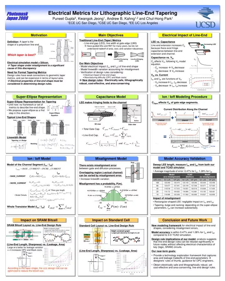
Vth Cg Increasing LEE LW0 LEG Poly r Active • Model Details Whole Transistor Model (Ion / Ioff) Electrical Metrics for Lithographic Line-End TaperingPuneet Gupta3, Kwangok Jeong1, Andrew B. Kahng1,2 and Chul-Hong Park11ECE UC San Diego, 2CSE UC San Diego, 3EE UC Los Angeles Motivation Main Objectives Electrical Impact of Line-End • Traditional Line-End (Taper) Metrics • Line-end gap (LEG), line width at gate edge (LW0) • Have guided litho and RET for many years, but do not • understand tradeoff of area, cost, and variation-robustness • Our Main Objectives • Model electrical impact (Ion and Ioff) of line-end shape • Model linewidth variation accounting for misalignment • Verification of design rules considering: • Electrical impact of line-end shape • Manufacturing difficulty (OPC and Mask costs) • New design rules: Electrically safe, lithographically robust, cost-effective, and area-conserving Definition: A taper is the shape of a polysilicon line-end. LEE vs. Capacitance Line-end extension increases Cg because there exist fringe capacitance between line-end extension and channel. Capacitance vs. Vth Cg affects Vth, following Vth model equation. - Cg increase Vth decrease - Cg decrease Vth increase Vth vs. Current Ion and Ioff are functions of Vth - Vth increase Ion, Ioff decrease - Vth decrease Ion, Ioff increase Which taper is best? Electrical simulation model Silicon. Taper shape under misalignment is a significant cause of this discrepancy Need for Formal Tapering Metrics Design rules have weak connections to geometric taper metrics, and can be expensive in terms of layout area. Electrical properties of line-end shape must be considered in determining design rules. Line-End Shortening (LES) Line-End Bridging (LEB) Super-Ellipse Representation Capacitance Model Ion / Ioff Modeling Procedure • Super-Ellipse Representation for Tapering • Until now: no framework or set of • metrics to describe line-end shape. • We propose super-ellipse as a first • step in this direction. LEE makes fringing fields to the channel CTaper affects Vth of gate edge segments. Current Distribution Along the Channel i i i Super-Ellipse Equation + + 0 Typical Line-End Shapes 0 0 channel channel channel Incremental current due to top LEE Current without LEE effect Incremental current due to bottom LEE • Total Gate Cap. top LEE = • Line-End Cap. S G D Linewidth Model Tapering and Bulge bottom LEE … Necking Cut line Cross-section view Ion / Ioff Model Misalignment Model Model Accuracy Validation Model of the Channel Segment (ion / ioff) • Sweep LEE length, measure Ion and Ioff from both our model and TCAD simulator. • Average magnitude of error: 0.47% for Ion, 1.28% for Ioff • There exists misalignment error between gate and diffusion processes. • Overlapping region (=actual channel) can be varied by misalignment error. • Increase linewidth variation ion ioff • BASE_CURRENT • INCRE_CURRENT Misalignment has a probability, P(m). • Impact of misalignment • Rectangular-shaped LEE: negligible impact on Ion and Ioff • Tapering, bulge and necking: depending on the super-ellipse • parameters, Ioff can increase substantially. Impact on SRAM Bitcell Impact on Standard Cell Conclusion and Future Work SRAM Bitcell Layout vs. Line-End Design Rule Standard Cell Layout vs. Line-End Design Rule • New modeling framework for electrical impact of line-end shapes, considering misalignment errors. • Model accuracy is within 0.47% and 1.28% for Ion and Ioff, compared to 3-D TCAD simulation. • Design rule implications of our model: analysis suggests that line-end design rules can be relaxed significantly in future nodes without affecting electrical characteristics of key (logic, SRAM) circuits. • Our near-term goals: • Provide a technology exploration framework that captures area and leakage tradeoffs of line-end parameters designers’ rules of thumb, guidance for OPC engineers. • Obtain electrically safe and lithographically robust, yet cost-effective and area-conserving, line-end design rules. (Line-End Length, Sharpness) vs. (Leakage, Area) Large n is better for leakage variation it increases OPC and Mask costs. (Line-End Length, Sharpness) vs. (Leakage, Area) According to the taper shape, the LEE design rule can be optimized to reduce the bitcell size.