Download
1 / 31
310 likes | 312 Views
This report outlines the progress and plans of the RD50 collaboration in developing radiation-hard semiconductor devices for high-luminosity colliders. It highlights the challenges faced, results obtained in 2005, and the work plan for 2006. The report also includes a list of collaborating institutes and the scientific strategies employed in the research.

E N D
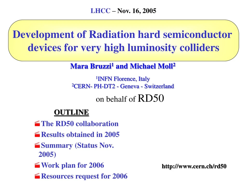
LHCC – Nov. 16, 2005 Development of Radiation hard semiconductor devices for very high luminosity colliders on behalf of RD50 Mara Bruzzi1 and Michael Moll21INFN Florence, Italy 2CERN- PH-DT2 - Geneva - Switzerland OUTLINE • The RD50 collaboration • Results obtained in 2005 • Summary (Status Nov. 2005) • Work plan for 2006 • Resources request for 2006 http://www.cern.ch/rd50
The CERN RD50 Collaborationhttp://www.cern.ch/rd50 RD50: Development of Radiation Hard Semiconductor Devices for High Luminosity Colliders • formed in November 2001 • approved as RD50 by CERN June 2002 • Main objective: Development of ultra-radiation hard semiconductor detectors for the luminosity upgrade of the LHC to 1035 cm-2s-1 (“Super-LHC”). Challenges: - Radiation hardness up to 1016 cm-2 required - Fast signal collection (Going from 25ns to 10 ns bunch crossing ?) - Low mass (reducing multiple scattering close to interaction point) - Cost effectiveness (big surfaces have to be covered with detectors!) • Presently 260 members from 53 institutes Belarus (Minsk), Belgium (Louvain), Canada (Montreal), Czech Republic (Prague (3x)), Finland (Helsinki, Lappeenranta), Germany (Berlin, Dortmund, Erfurt, Freiburg, Hamburg, Karlsruhe, Munich), Israel (Tel Aviv), Italy (Bari, Bologna, Florence, Padova, Perugia, Pisa, Trento, Turin), Lithuania (Vilnius), Norway (Oslo (2x)), Poland (Warsaw(2x)), Romania (Bucharest (2x)),Russia (Moscow), St.Petersburg), Slovenia (Ljubljana), Spain (Barcelona, Valencia), Switzerland (CERN, PSI), Ukraine (Kiev), United Kingdom(Exeter, Glasgow, Lancaster, Liverpool, Oxford, Sheffield, Surrey), USA (Fermilab, Purdue University, Rochester University, SCIPP Santa Cruz, Syracuse University, BNL, University of New Mexico) Mara Bruzzi and Michael Moll on behalf of the RD50 CERN Collaboration – LHCC, November 16, 2005 -2-
Scientific Organization of RD50Development of Radiation Hard Semiconductor Devices for High Luminosity Colliders Spokespersons Mara Bruzzi, Michael Moll INFN Florence, CERN ECP Defect / Material CharacterizationBengt Svensson(Oslo University) Defect EngineeringEckhart Fretwurst(Hamburg University) New MaterialsE: Verbitskaya(Ioffe St. Petersburg) Pad DetectorCharacterizationG. Kramberger(Ljubljana) New StructuresR. Bates (Glasgow University) Full DetectorSystemsGianluigiCasse (Liverpool University) Characterization of microscopic properties of standard-, defect engineered and new materials pre- and post-irradiation DLTS Calibration (B.Svensson) • Development and testing of defect engineered silicon: • - Epitaxial Silicon • - High res. CZ, MCZ • - Other impuritiesH, N, Ge, … • - Thermal donors • - Pre-irradiation • Oxygen Dimer (M.Moll) Development of new materials with promising radiation hard properties: - bulk, epitaxial SiC - GaN - other materials GaN (J.Vaitkus) • Test structure characterization IV, CV, CCE • NIEL • Device modeling • Operational conditions • Common irrad. • Standardisation of macroscopic measurements (A.Chilingarov) • 3D detectors • Thin detectors • Cost effective solutions • 3D (M. Boscardin) • Semi 3D (Z.Li) • LHC-like tests • Links to HEP • Links to R&D of electronics • Comparison: pad-mini-full detectors • Comparison of detectors different producers (Eremin) • pixel group (D. • Bortoletto,T. Rohe) Mara Bruzzi and Michael Moll on behalf of the RD50 CERN Collaboration – LHCC, November 16, 2005 -3-
Approaches to develop radiation harder tracking detectors Scientific strategies: • Material engineering • Device engineering • Change of detectoroperational conditions • Defect Engineering of Silicon • Understanding radiation damage • Macroscopic effects and Microscopic defects • Simulation of defect properties & kinetics • Irradiation with different particles & energies • Oxygen rich Silicon • DOFZ, Cz, MCZ, EPI • Oxygen dimer & hydrogen enriched Si • Pre-irradiated Si • Influence of processing technology • New Materials • Silicon Carbide (SiC), Gallium Nitride (GaN) • Diamond: CERN RD42 Collaboration • Device Engineering (New Detector Designs) • p-type silicon detectors (n-in-p) • thin detectors • 3D and Semi 3D detectors • Stripixels • Cost effective detectors • Simulation of highly irradiated detectors • Monolithic devices CERN-RD39“Cryogenic Tracking Detectors” Mara Bruzzi and Michael Moll on behalf of the RD50 CERN Collaboration – LHCC, November 16, 2005 -4-
Silicon Materials under Investigation by RD50 • CZ silicon: • high Oi (oxygen) and O2i (oxygen dimer) concentration (homogeneous) • formation of shallow Thermal Donors possible • Epi silicon • high Oi , O2i content due to out-diffusion from the CZ substrate (inhomogeneous) • thin layers: high doping possible (low starting resistivity) Mara Bruzzi and Michael Moll on behalf of the RD50 CERN Collaboration – LHCC, November 16, 2005 -5-
…. with time (annealing): 80 min 60C • Leakage current decreasing in time (depending on temperature) • Strong temperature dependence Consequence: Cool detectors during operation! Example: I(-10°C) ~1/16 I(20°C) Radiation Damage – I. Leakage Current • Change of Leakage Current (after hadron irradiation)…. with particle fluence: 80 min 60C • Damage parameter (slope in figure) Leakage current per unit volume and particle fluence • is constant over several orders of fluenceand independent of impurity concentration in Si can be used forfluence measurement Mara Bruzzi and Michael Moll on behalf of the RD50 CERN Collaboration – LHCC, November 16, 2005 -6-
…. with time (annealing): • Short term: “Beneficial annealing”• Long term: “Reverse annealing” - time constant depends on temperature:~ 500 years (-10°C)~ 500 days ( 20°C)~ 21 hours ( 60°C) - Consequence: Detectors must be cooled even when the experiment is not running! Radiation Damage – II. Effective doping concentration • Change of Depletion Voltage Vdep (Neff)…. with particle fluence: •“Type inversion”: Neff changes from positive to negative (Space Charge Sign Inversion) Mara Bruzzi and Michael Moll on behalf of the RD50 CERN Collaboration – LHCC, November 16, 2005 -7-
Standard FZ, DOFZ, Cz and MCz Silicon 24 GeV/c proton irradiation • Standard FZ silicon • type inversion at ~ 21013 p/cm2 • strong Neff increase at high fluence • Oxygenated FZ (DOFZ) • type inversion at ~ 21013 p/cm2 • reduced Neff increase at high fluence • CZ siliconand MCZ silicon • no type inversion in the overall fluence range donor generation overcompensates acceptor generation in high fluence range • Common to all materials: • same reverse current increase • same increase of trapping (electrons and holes) within ~ 20% Mara Bruzzi and Michael Moll on behalf of the RD50 CERN Collaboration – LHCC, November 16, 2005 -8-
EPI Devices 105V (25mm) 230V (50mm) 320V (75mm) • Epitaxial silicon grown by ITME • Layer thickness: 25, 50, 75 m; resistivity: ~ 50 cm • Oxygen: [O] 91016cm-3; Oxygen dimers (detected via IO2-defect formation) G.Lindström et al.,10th European Symposium on Semiconductor Detectors, 12-16 June 2005 • No type inversion in the full range up to ~ 1016 p/cm2 and ~ 1016 n/cm2 (type inversion only observed during long term annealing) • Proposed explanation: introduction of shallow donors bigger than generation of deep acceptors Mara Bruzzi and Michael Moll on behalf of the RD50 CERN Collaboration – LHCC, November 16, 2005 -9-
Annealing after proton irradiation n-type MCz silicon 300mm n- and p-type MCz vs FZ Si 300mm G. Segneri et al., presented at the Liverpool Conference, Sept. 2005 M. Scaringella et al., presented at the RD05 Conference, Florence, Oct. 2005 Effect of reverse annealing significantly reduced in MCz Si after irradiation with 26MeV and 24GeV/c up to 2x10¹⁵ 1MeV cm-2 with respect to FZ Si. Mara Bruzzi and Michael Moll on behalf of the RD50 CERN Collaboration – LHCC, November 16, 2005 -10-
Detector withcooling when notoperated Detector withoutcooling when notoperated Damage Projection – SLHC - 50 mm EPI silicon: a solution for pixels ?- G.Lindström et al.,10th European Symposium on Semiconductor Detectors, 12-16 June 2005 (Damage projection: M.Moll) Example: EPI 50 µm, Φp = 1.01·1016 cm-2 • Radiation level (4cm): eq(year) = 3.5 1015 cm-2 • SLHC-scenario: 1 year = 100 days beam (-7C) 30 days maintenance (20C) 235 days no beam (-7C or 20C) G. Lindstroem et al., 7th RD50 Workshop, Nov. 14-16, 2005 Mara Bruzzi and Michael Moll on behalf of the RD50 CERN Collaboration – LHCC, November 16, 2005 -11-
Characterization of microscopic defects - g and proton irradiated silicon detectors - • 2003: Major breakthrough on g-irradiated samples • For the first time macroscopic changes of the depletion voltage and leakage currentcan be explained by electrical properties of measured defects ! • 2005: Shallow donors generated by irradiation in MCz Si and epitaxial silicon after proton irradiation observed [APL, 82, 2169, March 2003] [G. Lindstroem, RD50 Workshop, Nov..2005] [D. Menichelli, RD50 Workshop, Nov..2005] Levels responsible for depletion voltage changes after proton irradiation: Almost independent of oxygen content: • Donor removal • “Cluster damage” negative chargeInfluenced by initial oxygen content: • I–defect: deep acceptor level at EC-0.54eV (good candidate for the V2O defect) negative charge Influenced by initial oxygen dimer content (?): • BD-defect: bistable shallow thermal donor (formed via oxygen dimers O2i) positive charge MCz n-type 26 MeV p irradiated, F=4×1014 cm-2 Epi 50mm 23 GeV p irradiated, F=4×1014 cm-2 BD-defect Mara Bruzzi and Michael Moll on behalf of the RD50 CERN Collaboration – LHCC, November 16, 2005 -12-
Radiation Damage – III.Decrease of CCE • Two basic mechanisms reduce collectable charge: • trapping of electrons and holes (depending on drift and shaping time !) • under-depletion (depending on detector design and geometry !) • Example: ATLAS microstrip detectors + fast electronics (25ns) • n-in-n versus p-in-n - same material, ~ same fluence- over-depletion needed • p-in-n : oxygenated versus standard FZ- beta source- 20% charge loss after 5x10¹⁴ p/cm2 (23 GeV) Mara Bruzzi and Michael Moll on behalf of the RD50 CERN Collaboration – LHCC, November 16, 2005 -13-
Process of segmented Si sensors Development of MCz & FZ Si n- and p-type microstrip/pixel sensors Two runs 20 wafers each 4” mini-strip 0.6x4.7cm2, 50 and 100mm pitch, AC coupled 37 pad diodes and various text structures P-type: two p-spray doses 3E12 amd 5E12 cm-2 Wafers processed by IRST, Trento on 200-500mm C. Piemonte, 5th RD50 workshop, Helsinki, Oct. 2004 n-type MCZ and FZ Si Wafers processed by SINTEF 300mm Within USCMS forward pixel project Thin microstrip detectors on 150-200-300mm thick processed by Micron Semiconductor L.t.d (UK) Micron will produce by the end of the year the microstrips on 300mm and 140mm thick 4” p-type FZ and DOFZ Si. D. Bortoletto, 6th RD50 workshop, Helsinki, June 2005 G. Casse, discussion of FDS, 7th RD50 workshop, Nov. 2005 Mara Bruzzi and Michael Moll on behalf of the RD50 CERN Collaboration – LHCC, November 16, 2005 -14-
n-in-p microstrip detectors n-in-p: - no type inversion, high electric field stays on structured side - collection of electrons • Miniature n-in-p microstrip detectors (280mm) • Detectors read-out with LHC speed (40MHz) chip (SCT128A) • Material: standard p-type and oxygenated (DOFZ) p-type • Irradiation: G. Casse et al., NIMA535(2004) 362 At the highest fluence Q~6500e at Vbias=900V CCE ~ 30% after 7.5 1015 p cm-2 900V (oxygenated p-type) CCE ~ 60% after 3 1015 p cm-2 at 900V( standard p-type) Mara Bruzzi and Michael Moll on behalf of the RD50 CERN Collaboration – LHCC, November 16, 2005 -15-
Annealing of p-type sensors • p-type strip detector (280mm) irradiated with 23 GeV p (7.5 1015 p/cm2 ) • expected from previous CV measurement of Vdep:- before reverse annealing:Vdep~ 2800V- after reverse annealingVdep > 12000V • no reverse annealing visible in the CCE measurement ! G.Casse et al.,10th European Symposium on Semiconductor Detectors, 12-16 June 2005 Mara Bruzzi and Michael Moll on behalf of the RD50 CERN Collaboration – LHCC, November 16, 2005 -16-
Charge Collection Efficiency in epitaxial Si • CCE measured with 244Cm -particles (5.8 MeV, R30 µm)Integration time window 20 ns • CCE degradation linear with fluence if the devices are fully depletedCCE = 1 – , = 2.710-17 cm2 CCE(1016 cm-2) = 70 % G. Lindstroem et al., 7th RD50 Workshop, Nov. 14, 2005 • CCE measured with 90Sr electrons (mip’s), shaping time 25 ns • CCE no degradation at low temperatures ! CCE measured after n- and p-irradiation CCE(Φp=1016 cm-2) = 2400 e (mp-value) trapping parameters = thos for FZ diodes for small Φ, For large Φ less trapping than expected ! See: G. Kramberger et al, NIM A, in press Mara Bruzzi and Michael Moll on behalf of the RD50 CERN Collaboration – LHCC, November 16, 2005 -17-
Sensor Materials: SiC and GaN • Wide bandgap (3.3eV) • lower leakage current than silicon • Signal:Diamond 36 e/mmSiC 51 e/mmSi 89 e/mm • more charge than diamond • Higher displacement threshold than silicon • radiation harder than silicon (?) R&D on diamond detectors:RD42 – Collaborationhttp://cern.ch/rd42/ Recent review: P.J.Sellin and J.Vaitkus on behalf of RD50 “New materials for radiation hard semiconductor detectors”, submitted to NIMA Mara Bruzzi and Michael Moll on behalf of the RD50 CERN Collaboration – LHCC, November 16, 2005 -18-
Epitaxial SiC: after irradiation p+/n diodes. Produced by Perugia on IKZ Berlin 50 mepitaxial layers • CCE before irradiation • 100 % with a particles and MIPS • tested thickness up 50mm • CCE after irradiation • with MIP particles • neutron irradiated samples • material produced by CREE • 50 mm thick layer [F. Moscatelli et al., presented at IEEE-NSS MIC Puerto Rico, 2005 ] Radiation damage has no negative effect on leakage current.For fluences above 3 ×10¹⁵ n/cm2 the signal is lower than 400 e- Mara Bruzzi and Michael Moll on behalf of the RD50 CERN Collaboration – LHCC, November 16, 2005 -19-
n n n p p n n n Device Engineering: 3D detectors • Electrodes: • narrow columns along detector thickness-“3D” • diameter: 10mm distance: 50 - 100mm • Lateral depletion: • lower depletion voltage needed • thicker detectors possible • fast signal • Hole processing : • Dry etching, Laser drilling, Photo Electro Chemical • Present aspect ratio (RD50) 30:1 (Introduced by S.I. Parker et al., NIMA 395 (1997) 328) • 3D detector developments within RD50: 1) Glasgow University – pn junction & Schottky contacts Irradiation tests up to 5x10¹⁴ p/cm2 and5x1014p/cm2: Vfd = 19V (inverted); CCE drop by 25% (a-particles) 2) IRST-Trento and CNM Barcelona (since 2003) CNM: Hole etching (DRIE); IRST: all further processing diffused contacts or doped polysilicon deposition Mara Bruzzi and Michael Moll on behalf of the RD50 CERN Collaboration – LHCC, November 16, 2005 -20-
3D Detectors: New Architecture Plan for 2005 • Simplified 3D architecture • n+ columns in p-type substrate, p+ backplane • operation similar to standard 3D detector • Simplified process • hole etching and doping only done once • no wafer bonding technology needed • Fabrication planned for end 2005 • INFN/Trento funded project: collaboration between IRST, Trento and CNM Barcelona • Simulation • CCE within < 10 ns • worst case shown(hit in middle of cell) 10ns [C. Piemonte et al., NIM A541 (2005) 441] Mara Bruzzi and Michael Moll on behalf of the RD50 CERN Collaboration – LHCC, November 16, 2005 -21-
ionizing particle cross-section between two electrodes n+ n+ holes drift in the central region and diffuse towards p+ contact electrons are swept away by the transversal field STC-3D detectors - by IRST-Trento [C. Piemonte et al, Nucl. Instr. Meth. A 541 (2005)] Functioning: Sketch of the detector: n+-columns p-type substrate grid-like bulk contact Adv. over standard 3D: etching and column doping performed only once Mara Bruzzi and Michael Moll on behalf of the RD50 CERN Collaboration – LHCC, November 16, 2005 -22-
10 m Hole depth: 120μm Fabrication process in 2005 metal MAIN STEPS: 1. Hole etching withDeep RIE machine (step performed at CNM, Barcelona, Spain) 2. n+ diffusion (column doping) 3. passivation of holes with oxide 4. contact opening 5. metallization oxide hole contact n+ diffusion • CHOICES FOR THIS PRODUCTION: • No hole filling (with polysilicon) • Holes are not etched all through the wafer • Bulk contact provided by a uniform p+ implant Mara Bruzzi and Michael Moll on behalf of the RD50 CERN Collaboration – LHCC, November 16, 2005 -23-
Mask layout “Large” strip-like detectors Small version of strip detectors Planar and 3D test structures “Low density layout” to increase mechanical robustness of the wafer Mara Bruzzi and Michael Moll on behalf of the RD50 CERN Collaboration – LHCC, November 16, 2005 -24-
Strip detectors – layout Inner guard ring (bias line) metal p-stop hole Contact opening n+ Mara Bruzzi and Michael Moll on behalf of the RD50 CERN Collaboration – LHCC, November 16, 2005 -25-
p-stop p-spray 30 25 20 Detectors count 15 10 Bias line Guard ring 5 0 >50 0 5 25 30 35 10 15 20 40 45 50 I bias line [nA] Strip detectors – IV measurements Average leakage current per column < 1pA Number of columns per detector: 12000 - 15000 Current distribution @ 40V of 70 different devices Leakage current < 1pA/column in most of the detectors Good process yield Mara Bruzzi and Michael Moll on behalf of the RD50 CERN Collaboration – LHCC, November 16, 2005 -26-
- Status 2005 ( I )- • At fluences up to 1015cm-2(Outer layers of a SLHC detector) the change of the depletion voltage and the large area to be covered by detectors is the major problem. • CZ silicon detectors could be a cost-effective radiation hard solution (no type inversion, use p-in-n technology) • oxygenated p-type silicon microstrip detectors show very encouraging results:CCE 6500 e; Feq=41015 cm-2, 300mm • No reverse annealing visible in the CCE measurement in 300mm-thick p-type FZ Si detectors irradiated with 24GeV p up to 7x1015cm-2 if applied voltage 500-800V. • n- and p-type MCz Si show reduced reverse annealing than FZ Si. • n-MCz Si not type inverted up to a 23GeV proton fluence of 2x1015cm-2. • New Materials like SiC and GaN (not shown) have been characterized. Tests made on SiC up to 1016cm-2 showed that detectors suffer no increase of leakage current but CCE degrade significantly. Maximum thickness tested: 50mm. Mara Bruzzi and Michael Moll on behalf of the RD50 CERN Collaboration – LHCC, November 16, 2005 -27-
- Status 2005 ( II )- • At the fluence of 1016cm-2 (Innermost layer of a SLHC detector) the active thickness of any silicon material is significantly reduced due to trapping. • The two most promising options so far are: • Thin/EPI detectors : drawback: radiation hard electronics for low signals needed • no reverse annealing – room T maintenance beneficial • thickness tested: up to 75mm. • CCE measured with 90Sr e, shaping time 25 ns, 75mm • Φp=1016 cm-2 = 2400 e (mp-value) • processing of 150mm n-epi and p-epi under way • 3D detectors: process performed at IRST-Trento of 3D-sct in 2005 • feasibility of 3D-stc detectors • Low leakage currents (< 1pA/column) • Breakdown @ 50V for p-spray and >100V for p-stop structures • Good process yield (typical detector current < 1pA/column) Mara Bruzzi and Michael Moll on behalf of the RD50 CERN Collaboration – LHCC, November 16, 2005 -28-
Workplan for 2006 (1/2) • Characterization of irradiated silicon: • Understand role of defects in annealing of p- and n-type MCz vs FZ Si • Continue study of influence of oxygen dimers on radiation damage • Extend studies to neutron irradiated MCz & FZ Si • Processing of High resistivity n- and p-type MCZ-silicon • Processing of epitaxial silicon layers of increased thickness • Hydrogenation of silicon detectors • Optimization of oxygen-dimer enriched silicon • Characterization (IV, CV, CCE witha- and b-particles) of test structures produced with the common RD50 masks • Common irradiation program with fluences up to 1016cm-2 • Significant radiation damage observed in SiC limited efforts to study possible improvements in material/geometry Defect and MaterialCharacterization Defect Engineering Pad DetectorCharacterization New Materials Mara Bruzzi and Michael Moll on behalf of the RD50 CERN Collaboration – LHCC, November 16, 2005 -29-
Workplan for 2006 (2/2) • Production of 3D detectors made with n+ and p+ columns • Measurement of charge collection before and after irradiation of the processed 3D detectors • Production of thinned detectors (50-200mm) wih low resistivity n-type FZ and MCZ Si. Comparison with epitaxial layers to fast hadron fluences of 1016cm-2 • Production, irradiation and test of common segmented structurescontinues (n- and p-type FZ, DOFZ, MCz and EPI) on 4” and 6” • Measurement of S/N on segmented sensors irradiated in 2005 • Investigation of the electric field profile in irradiated segmented sensors • Continue activities linked to LHC experiments New Structures Full Detector Systems Mara Bruzzi and Michael Moll on behalf of the RD50 CERN Collaboration – LHCC, November 16, 2005 -30-
Resources requested for 2006 • Common Fund: RD50 has a Common Fund and does not request financial support. • Lab space and technical support at CERN:As a member of the collaboration, the section PH-DT2/SD should provide (as in 2005) access to available lab space in building 14 (characterization of irradiated detectors), in building 28 (lab space for general work) and in the Silicon Facility (hall 186, clean space). • CERN Infrastructure:- One collaboration workshop in November 2006 and working group meetings.- Keeping the RD50 office in the barrack 591 Mara Bruzzi and Michael Moll on behalf of the RD50 CERN Collaboration – LHCC, November 16, 2005 -31-