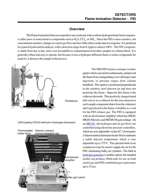
Download
1 / 35
350 likes | 364 Views
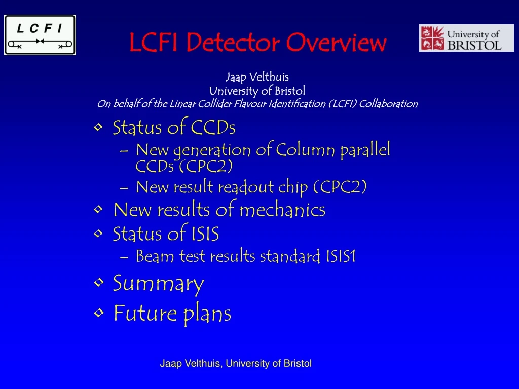
LCFI Detector Overview. Jaap Velthuis University of Bristol On behalf of the Linear Collider Flavour Identification (LCFI) Collaboration. Status of CCDs New generation of Column parallel CCDs (CPC2) New result readout chip (CPC2) New results of mechanics Status of ISIS

E N D
LCFI Detector Overview Jaap Velthuis University of Bristol On behalf of the Linear Collider Flavour Identification (LCFI) Collaboration • Status of CCDs • New generation of Column parallel CCDs (CPC2) • New result readout chip (CPC2) • New results of mechanics • Status of ISIS • Beam test results standard ISIS1 • Summary • Future plans Jaap Velthuis, University of Bristol
PCB based transformer CCD abbreviations Column Parallel Readout Chip (CPRxx) Column parallel CCD (CPCCDx or even CPCx) CPD=clock driver Jaap Velthuis, University of Bristol
CPC2-70 104 mm CPC2-40 CPC2-10 Second Generation CPCCD : CPC2 • CPC2 wafer (100 .cm/25 μm epi and 1.5k.cm/50 μm epi) • Low speed (single level metallisation) and high speed versions • High speed (busline-free) devices with 2-level metal clock distribution: • The whole image area serves as a distributed busline • Designed to reach 50 MHz operation (needed to keep the occupancy < 1% in L1) Jaap Velthuis, University of Bristol
55Fe source removed X-ray hits Transformer drive CCD output (2-stage source follower), 2 Vpk-pk clocks CPC2 – High Speed in Stand-alone Mode • First tests with a PCB transformer and a RF amplifier for clocking • Busline-free CPC2-10 working at 45 MHz, important milestone • Numerous parasitics diminish overall performance, high noise from the RF amplifier • CMOS driver chip used as well K.Stefanov, RAL B.Hawes, Oxford Jaap Velthuis, University of Bristol
10 MHz System noise = 75 e- RMS CPC2-10 BLF with CPD1 Clocking • 55Fe signal (1620 electrons, MIP-like) • CPD1 producing 20 A clocks in the range 3.3 V to 1.2 V • Tests are continuing – pushing up frequency, using 50 mm long sensor • Main limitation for high frequency: ground bounce coursed by clock K.Stefanov Y.Li Jaap Velthuis, University of Bristol
Readout Chips – CPR1 and CPR2 Both 0.25 μm CMOS process (IBM) Front-end amplifiers matched CCD CPR1 can be bump-bonded to CPC1 and CPC2, also has 1-in-3 wire bondable pads CPR2 can only be bump-bonded to CPC2 Additional test features in CPR2 Voltage and charge amplifiers 125 channels each Analogue test I/O Digital test I/O 5-bit flash ADCs on 20 μm pitch Cluster finding logic (22 kernel) Sparse readout circuitry FIFO Bump bond pads CPR1 CPR2 Wire/Bump bond pads S.Thomas Jaap Velthuis, University of Bristol
CPR2: Analogue Performance • Bump-bonded CPC2/CPR2 driven by two CPD1 chips • Noise around 60 e • Works up to 9 MHz X-ray signal Signal histogram Jaap Velthuis, University of Bristol
New Features in CPR2A • Improvements implemented in CPR2A: • Cluster size reduced to 46 • 3-fold increase in the column memory buffer (can store up to 3 clusters) to reduce dead time and a new state machine • Individual column threshold – corrects for gain variations • Analogue calibration circuit – the chip can be partially tested without bump bonding to a CCD • Improvements to the analogue circuitry: gain matching, reduced differential non-linearity in the ADC, new clock distribution • Digital crosstalk to the charge amplifiers will be minimized • Code-dependent current in the ADC will be reduced • CPR2A received in May, tests started Jaap Velthuis, University of Bristol
CPR2A Tests • CPR2A received in May, tests started • ADC tests with calinjects – works OK Jaap Velthuis, University of Bristol
CPC-T • Two-fold goal : lower V and lower C • Two designs based on CPC2 to study very low inter-gate barriers and clock amplitudes • Six designs for reduction of the inter-gate capacitance: • Pedestal CCD (on 20 m and 24 m pitch) • Shaped Channel CCD (variant of the Pedestal CCD), on 20 m and 24 m pitch • Open Phase CCD • “Inter-channel gap” CCD • Pedestal designs could reduce Cig by a factor of 2-4, open phase by 2 Jaap Velthuis, University of Bristol
CPC-T • 6 CPC-T wafers delivered, one of each type • One type (stepped nitride barrier) failed the complete wafer • Tests started at RAL and Oxford – the chip works! • First results at 50 MHz with 4-phase CPCCD, studies of minimal voltages Jaap Velthuis, University of Bristol
Mechanical Studies • To make stiff light weight structures are studying SiC foams • CCDs need significant cooling Jaap Velthuis, University of Bristol
Mechanical Studies Jaap Velthuis, University of Bristol
Status of ISIS • In-Situ Image Sensor • Beam test of ISIS1 • Noise & Signals • Tracks • Position resolution • Efficiency Jaap Velthuis, University of Bristol
In-Situ Image Sensor • Operational Principles: • Every pixel has mini CCD to store charge: burst camera with multiframes • Charge collected at photogate • Transferred to storage pixel during bunch train • 20 transfers per 1ms bunch train • Readout during 200ms quiet period after bunch train Jaap Velthuis, University of Bristol
ISIS properties and status • ISIS advantages • Low frequency clock -> easy to drive • 20 kHz during capture, 1MHz readout • ~100 times more radiation hard than CCDs (fewer charge transfers) • Conversion to voltage and readout in the 200 ms-long quiet period after the train, RF pickup is avoided • ISIS combines CCDs, active pixel transistors and edge electronics in one device • “Proof of principle” device (ISIS1) designed and manufactured by e2V Technologies • ISIS2 submitted 2 weeks ago Jaap Velthuis, University of Bristol
OG RG OD RSEL Column transistor OUT ISIS1 • 1616 array of ISIS1 cells with 5-pixel buried channel CCD storage register each • Cell pitch 40 μm 160 μm, no edge logic (pure CCD process) • Total active area 0.56×2.24mm2 Output and reset transistors Photogate Aperture (8 μm square) CCD (56.75 μm pixels) Jaap Velthuis, University of Bristol
sense node (n+) reset gate output gate storage pixel #1 transfer gate storage pixel #5 VDD row select isolation gate photogate To column load buried channel (n) p+ well reflected charge Charge collection reflected charge High resistivity epitaxial layer (p-) substrate (p++) ISIS1 (II) • ISIS1 comes in two versions. Standard and p-well. P-well ISIS has entire buried channel in p+-well. All results here on std ISIS1 P-well not present std ISIS1 Jaap Velthuis, University of Bristol
preliminary ISIS1 works! • Here S/N all pixels all events, pedestal corrected, spectrum Fe55 different settings for timing and photogate voltage as in beam test Jaap Velthuis, University of Bristol
ISIS1 with p-well • High p-well doping protect storage register • Look at ratio R of charge collected at photogate to charge collected at storage pixel • If increase clock voltage, get punchthrough under in-pixel CCD, R drops • Lower p-well doping, charge reflection decreases • No p-well, R ~ 7 • dependent on gate geometry and voltages • All results after using standard ISIS1 without p+-well K.Stefanov G.Zhang, RAL Jaap Velthuis, University of Bristol
Beam test • Beam test October-November 2007 • DESY 1…6 GeV e- • Self contained ISIS telescope • 5 ISIS in a row • Readout speed 2.5 MHz • for ILC need only 1 MHz Jaap Velthuis, University of Bristol
Beam test preparations • 16×16 pixels each 40×160μm2 • Total active area 0.56×2.24mm2 • Needed precision mounting Jaap Velthuis, University of Bristol
Noise 2D Noise 1D Pedestal preliminary preliminary preliminary Pedestals and Noise • For analysis each memory cell separate pixel i.e. 16x(16x5) • Calculate average offset for each pixel • Reiterate to remove hits • Random noise calculated as std dev after pedestal removal • No common mode found Jaap Velthuis, University of Bristol
preliminary preliminary preliminary η=Qright/(Qleft+Qright) Signals • Cluster cut • 5σ seed, 2σ next cut • Clusters small • Pitch 160 μm in X • Little charge sharing in X • η in Y demonstrates charge sharing • S/N=37.3±0.2 • Homogeneous memory cells • Lower peak due to local inefficient charge collection. Will come back later. Jaap Velthuis, University of Bristol
x(sensor) vs. x(sensor) y(sensor) vs. y(sensor) Tracks • Tracks result in correlations between hits in different ISIS sensors Jaap Velthuis, University of Bristol
Using η preliminary preliminary Position resolution • Using ISIS 0,1 and 3 to predict ISIS 2 • ση = 10.8± 0.3 μm • Homogeneous over memory cells • Includes tracking and multiple scattering error (large!: 4 devices 600μm thick, 6 GeV e-) • Doesn’t work X: • Pixels too large • Same in Y, but less pronounced Jaap Velthuis, University of Bristol
Efficiency • Efficiency measurement: • Take events with just 1 hit in telescope planes. • Fit track • Check whether hit found in DUT at correct place • Efficiency very low, but no surprise. • Pitch very large 160×40μm2 • Relying on diffusion • Not enough charge arriving, hence might miss hits too far away photo gate Jaap Velthuis, University of Bristol
Efficiency (II) • The problem occurs due to the very asymmetric pitch and large pitch. • Hit occurring worst position, difference in distance to the photo gates small. • From the geometry, need S/N of ~55 for 100% efficiency Jaap Velthuis, University of Bristol
100 e- 400 e- 200 e- Simple toy MC • Generate signals MPV 4000e- (50μm epi-layer) • Location randomly over pixel • Spread signal 5x5 area • Standard analysis (5σ seed and 2σ next) • Vary noise • Can get double peak Jaap Velthuis, University of Bristol
200e- 300e- 400e- 115e- Simple toy MC • Implementing some trapping proportional to distance yields even clearer double peaks • Qualitatively understand ISIS1 result and are happy: • ISIS concept works • S/N not too bad • Just pitch too large, hence poor efficiency Jaap Velthuis, University of Bristol
Cross section under Photogate ISIS2 • Jazz Semiconductor will manufacture ISIS2 • Process: 0.18 mm with dual gate oxide • Area 1 cm2 (four 5x5 mm2 tiles) • 32x128 pixels (x2 designs) • Developed buried channel and deep p+ implant • Buried channel is necessary for CCD • Deep p+ is beneficial to decouple buried channel from p-well, no need for punchthrough, was absent in ISIS1 Jaap Velthuis, University of Bristol
ISIS2 • Pixels 80 x 10 mm2 • Buried channel 5 mm wide • 20 memory cells • 3 metal layers • CCD gates: doped polysilicon • Staggered pixel layout, max distance to electrode 21 mm • Submitted end of Mai. Receive in October 2008 Jaap Velthuis, University of Bristol
Summary • Making a lot of progress on CCD development • Successfully operated a busline-free CPC2-10 at 45 MHz using a PCB transformer and a RF amplifier for clocking . Noise better than 150e- at 30MHz. • New readout chip CPR2A • Received in May. First tests (Charge injection in ADC) seems fine. • Improving CCD layout to reach lower V and lower C. Testing 6 new designs, tests just started, but chips work. • On mechanics side, SiC foam ladders perform very well. Stay well in shape over large temperature range Jaap Velthuis, University of Bristol
Summary (II) • Performed successful ISIS1 beam test • Demonstrated that ISIS concept works well as a sensor • Main results: • S/N=37.3±0.2 (for hits around photogate) • Can still improve S/N in current setup • Thinning to ILC thickness does not affect S/N • σ = 10.8± 0.4 μm • S/N and σ homogeneous over memory cells • Efficiency 66% (not so nice, but due to pitch) • Should be much better in newer ISIS design ISIS2 Jaap Velthuis, University of Bristol
Future plans • Continue to test new CCD structures. Try to improve the noise. • Further test new readout chip. • Further develop SiC-foam ladders. • For ISIS(1): • Build DAQ system with laser and X,Y motor stage to study local charge loss. • Planned ISIS1 beam test in August 2008 at CERN using EUDET telescope • more precise tracking • Measure signal and efficiency as function in-pixel position • Need to test and compare p-type ISIS1 • Eagerly awaiting ISIS2 Jaap Velthuis, University of Bristol