Download
1 / 17
170 likes | 256 Views
AIDA WP3 Summary. Status of milestones and deliverables Status of sub-projects Plans for the last year of AIDA. Objectives. Sub-Projects. WP3.2 (3D interconnection)

E N D
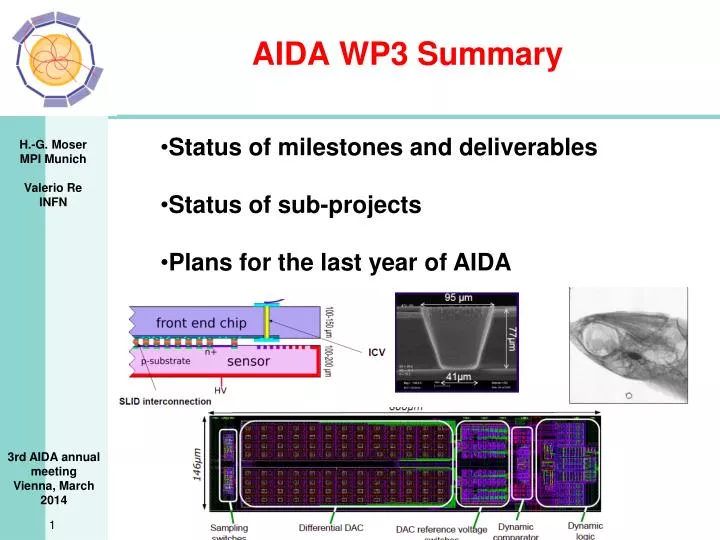
AIDA WP3 Summary • Status of milestones and deliverables • Status of sub-projects • Plans for the last year of AIDA
Sub-Projects • WP3.2 (3D interconnection) • Bonn/CPPM: Interconnection of the ATLAS FEI4 chips to sensors using bump bonding and TSVs from IZM (large diameter TSV, large interconnection pitch). • CERN: Interconnection of MEDIPIX3 chips using the CEA-LETI process • INFN/IPHC-IRFU: Interconnection of chips from Tezzaron/Chartered to edgeless sensors and/or CMOS sensors using an advanced interconnection process (T-MICRO or others) • LAL/LAPP/LPNHE/MPP: Readout ASICs in 65nm technology interconnected to pixel sensors using the CEA-LETI or EMFT process. • MPP/GLA/LAL/LIV/LPNHE:Interconnection of ATLAS FEI4 chips to sensors using SLID interconnection and ICV (high density TSVs) from EMFT. • UB: 3D interconnection of 2 layers of Geiger-Mode APD arrays with integrated readout in Tezzaron Chartered technology. • RAL/UPPSALA: Integration of a 2-Tier readout ASIC for a CZT pixel sensor using EMFT SLID technology and TSV including redistribution of I/O connections to the backside for a 4-side buttable device. • WP3.3 (IP blocks) • IP blocks in 65 nm CMOS (coordinated by CERN): The choice of the 65 nm CMOS generation wasprompted by the needs of future vertex detectors, which can benefit from modernnanoscaletechnologies by obtainingsmaller and more intelligentpixels in pixel detectors, more compact digitallogic and lowerpower in front-end chips. • IP blocks in SiGe (coordinated by LAL-CNRS): provide IP blocks for needs in calorimeters and TPCs. These two domains are demanding in high dynamic range and precision, so the choice of technology would be to use Silicon Germanium (SiGe).
Milestones post-poned Milestone achieved if some of the subprojects are successful
Deliverables postponed Deliverable achieved if some of the subprojects are successful
WP3.2: Bonn/CPPM 3D interconnection of sensor and ATLAS FEI4 chip with TSV in periphery => reduce dead area (final target: 4-side buttable) => post processing, to be applied at existing chip TSVs, RDL and bump bonding by Fraunhofer IZM Test with FEI2 successful (tapered vias) Process needs to be changed for FEI4 (no front side processing) Use optimized bonding process for thin chips (<100µm) To be processed this year Connected Not connected
WP3.2: MPP/GLA/LAL/LIV/LPNH • Interconnection of ATLAS FEI4 to thin, slim • edge sensors • 4 side buttalbe(Backside connectivity) • high TSV density (small diameter) • SLID interconnection and TSV by Fraunhofer EMFT • First SLID tests with FEI2 successful • TSVs etched, but problems with tungsten filling • FEI4 needs different TSV etching technology (fbackside) • Status • TSV design for FEI4 made • Dedicated sensors produced (CIS, VTT) • Plans • SLID interconnection FEI4/Sensor (w/o TSV) • Develop TSV process for FEI4 • SLID FEI4/sensor with TSV (if time allows)
WP3.2: LAL/LAPP/LPNHE/MPP 3D device based on OMEGAPIX with high density bonding (35µm x 200µm staggered: 70µm pitch ASIC: 2-tier OMAGAPIX2, by TEZZARON, ordered Oct 2011, delivered Jan 2014 first tests promising Interconnection: CEA-LETI with slim edge sensors by VTT and CIS (avialble) Alternative (no new TEZZARON run in sight): 2D version of OMEGAPIX in 65nm technology (by Europractice, CERN?) (wafers needed for interconnect) Submission this year
WP3.2: INFN/IPHC-IRFU Establish a procedure to interconnect small pixels (20µm x 20µm) at pixel level 2-tier stack (2 x 50µm) Pixel sensors in both layers Top tier read out via bottom tier Sensors processed in 180nm CIS technology (TowerJazz) Thinning & SLID interconnection by Fraunhofer IMS Status: 6 wafers being processed, expected in May Plans: SLID interconnection finished in November Test at IPHC: December top tier bottom tier test sensor
WP3.2: RAL/Uppsala Demonstrate a pixel readout chip with 2 tiers and TSVs in every pixel Tier 1 (analogue) based on RAL HEXITEC chip (X-ray imaging) Tier 2 (dgitial): 12 bit DAC and readout Thinning, TSVs and SLID interconnection by EMFT Fraunhofer (like MPP project) Some delays due to contract issues First wafers delivered in October 2013 (6 months delay) TSVs and RDL are generally ok SLID interconnection seems to be of poor quality Plans: Delivered devices will be tested EMFT agreed to produce more devices free of charge 12 wafers purchases and sent to EMFT Assembled wafers expected by June 2014
WP3.2: CERN 4-side buttable readout ASIC (based on Medipix) with TSV TSVs and RDL by CEA LETI (large diameter TSV, 60µm diam.) After TSV & thinning: chip performance unchanged Interconnection (bump bonding) by ADVACAM on edgeless sensors Sensor/chip assemblies work Next steps: Yield studies Ultrathin assemblies Using TIMEPIX (50µm & 50 µm)
WP3.3: 65nm IP blocks Contract with TSMC by CERN • Foundry access via IMEC • Long procedures for • Signature of NDA is imminent • Contract covers a period of 5 years (2013-2017) Rad hard IP blocks designed (CERN) • SRAM compiler • I/O pad library • Monitoring ADC • Bandgap reference • specified to 200Mrad Rad soft IP blocks designed (CERN) • 2C slave • HDLC communication protocol • 7b8b communication protocol
WP3.3: SiGe/SOI IP blocks • Electronics needs in calorimeters and TPCs : • large dynamic range, high speed, low noise, low offset, • need of precise capacitors and resistors, … • Blocks : • ADC, TDC, DAC, Bandgap, OTA, Rad-tol memory, SEU resistant flipflop … • Technology : SiGe or HV SOI • SiGe still moving a lot => shift to AIDA2 • Choose XFAB SOI 180 nm (SOI --> fast, low substrate noise, low cost, HV capability, latchup free) Chose XFAB 0.18 µm SOI process Possible run for blocks soumission : 22 September2014
WP3.3: Others AGH-UST Waiting for CERN 65nm contract In the meantime Two low power ADCs (6-bit, 10-bit), general purpose PLL and SLVS interface were designed in 130 nm, fabricated and tested. • All blocks are fully functional, quantitative tests show excellent results for 6-bit ADC and good results for 10-bit ADC and PLL. • Improved versions were submitted in February 2014 SACLAY: IP blocks desigend, to be submitteds (130 nm) 10-bit SAR ADC for Lumical
Next year’s objectives • WP3.2 • Deliverable D3.8: detectors available for 3D assessment • -> already achieved by CERN • Deliverable D3.10:Assemsent of 3D integrated sensors • -> push all subprojects to achieve deliverables • Assess performance of 3D sensors taking into account: • cost, processing time • technological challenges • experience with industry and vendors • recommendation for further R&D • WP3.3 • Deliverables D3.4 (postponed) and D3.9 • Prepare for final report