Download
1 / 13
130 likes | 230 Views
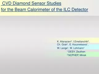
CVD Diamond Sensors for the Very Forward Calorimeter of a Linear Collider Detector. K. Afanaciev, D. Drachenberg, E. Kouznetsova, W. Lange, W. Lohmann. LCal at TESLA. Detection and measurement of electrons and photons at small angles Fast beam diagnostic

E N D
CVD Diamond Sensors for the Very Forward Calorimeter of a Linear Collider Detector K. Afanaciev, D. Drachenberg, E. Kouznetsova, W. Lange, W. Lohmann
LCal at TESLA • Detection and measurement of electrons and photons at small angles • Fast beam diagnostic • Shielding of the inner part of the detector • Backgroung : Beamstrahlung • Per bunch crossing : • ~15000 e± hit the LCAL • ~20 TeV of deposited energy • Expected dose : • for “bad” regions : • up to 10 MGy/year -> Radiation hard sensor -> diamond ?
Diamond samples • Fraunhofer Institute (Freiburg) : • CVD diamond 12 x 12 mm • 300 and 200 um thickness • Different surface treatment : • #1 – substrate side polished; 300 um • #2 – substrate removed; 200 um • #3 – growth side polished; 300 um • #4 – both sides polished; 300 um • Metallization: • 10 nm Ti + 400 nm Au • Area 10 X 10 mm Picture showing the difference b/w growth and substrate
HV Diamond Keithley 487 N2 I(V) dependence – setup Measurements were done with Keithly 487 picoammeter • Extremely low currents => N2 atmosphere EM shielding • Average resistance ~(1013-1014) Ohm (ohmic behavior) • 3 samples from different groups have “non-ohmic” behavior and lower resistance (~1011 Ohm) Usual I(V) curve Non-ohmic curve
ADC Sr90 delay PA diam. Scint. discr & PM1 Gate discr PM2 Charge Collection Distance (CCD) Qmeas. = Qcreated x ccd / L Qcreated(mm) = 36 e-h pairs • The samples haven’t been irradiated before these measurements • All data was taken 2 minutes after bias voltage applied
CCD – irradiation studies • The samples were irradiated with Sr-source with estimated dose-rate of about 0.45 Gray per hour • The total absorbed dose for all the samples was at least 5 Gy. • Bias field was set to 1 V/m • Irradiation was homogeneous over the sample area • Parameters monitored during the irradiation: • Sr-spectrum peak position • width of the peak (->noise) • current in HV-circuit • test pulse from a generator (-> electronics stability)
CCD – irradiation studies – results Group #2 (substrate side removed). HV = 200V Group #3 (growth side polished). HV = 300V
CCD – irradiation studies – results Group #2 (substrate side removed). HV = 200V Group #1 (substrate side polished). HV = 300V
CCD – irradiation studies – results Group #3 (growth side polished). HV = 300V Group #4 (both sides polished). HV = 300V
N (575) N (637) FAP 2_1 LO Phonon Si (770) FAP 4_2 Results and further studies • Raman spectroscopy + photoluminescence analysis -> no nitrogen, no silicon Reference spectra
Removed substrate • Group#3 – removed substrate (300 mm -> 240 mm)
Results and further studies • Group#2 in general can work as a detector • Raman spectroscopy + photoluminescence analysis -> no nitrogen, no silicon • Next steps: • Influence of the substrate side on CCD and stability • Homogeneity and linearity required for the application