Download
1 / 30
310 likes | 339 Views
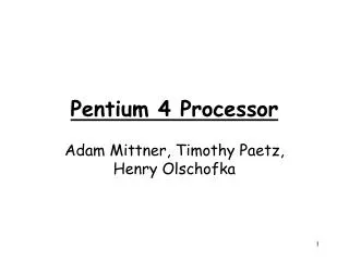
The Microarchitecture of the Pentium 4 processor. Glenn Hinton, Dave Sager, Mike Upton, Darrell Boggs, Doug Carmean, Alan Kyker, Patrice Roussel. Presented by : Ajay Sharma. System Bus. Level 1 Data cache. Bus Unit. Execution Unit. Level 2 Cache. Integer & FP Execution Units.

E N D
The Microarchitecture of the Pentium 4 processor Glenn Hinton, Dave Sager, Mike Upton, Darrell Boggs, Doug Carmean, Alan Kyker, Patrice Roussel. Presented by : Ajay Sharma
System Bus Level 1 Data cache Bus Unit Execution Unit Level 2 Cache Integer & FP Execution Units Memory Subsystem Fetch/ Decode Trace cache Out of order Execution Logic Retire ment BTB/Branch Prediction Branch History Update Out of order Engine Front End Overview of the Netburst™ Micro-Architecture
In-Order Front End • Fetches the Instructions, decode them and send them to the out of order execution core. • There are three parts to it: • Fetch/Decode Unit. • Execution Trace cache. • BTB/Branch Prediction
Out of Order Engine • This is where the Instructions are prepared for execution. • There are two parts to it: • Out of order Execution Logic -> Allows maximum Utilization • Retirement Unit -> Ensures that the Instruction are back in order.
Integer and Floating-Point Units • This is the Unit where the Instructions are actually executed. • It has two parts: • L-1 data cache • Execution Unit
Memory Subsystem • It does many things like store the Instructions in the Level 2 cache when the Trace cache and the L1 cache is filled. • It also is used to access the main memory when the L2 cache has a cache miss and the System I/O resources.
Clock Rates • Clock rates determine the stages of pipeline. • Higher clock rate actually require deeper pipeline and more time for cache miss and mispredicted branch. • But overall they are performance booster. • Say 50% increase in frequency results in only 30% increase in the Net Performance but that is still good.
Clocking trends • The clock rates have increased by 2.5 times from original in 286.
Misprediction Pipeline As the No of Pipeline increase we can do more work per clock and so the clock rate increases.
Front End BTB & Instruction TLB: Steer the front-end when a cache miss happens. ITLB translates the Linear address to physical address. Trace cache: Only decoded instructions are stored in this cache and when there is a mis-prediction there is no need to re-decode the instruction and so decode latency is reduced. Trace Cache BTB: The Instructions in the cache are predicted for branch taken/not taken. So that the delay can be reduced. Microcode ROM: This is used for complex instruction execution. µop Queue: This holds in-order µOPs from trace cache and microcode ROM before they are sent to the out-of-order execution unit. 1. Front End
Allocator: It attempts to allocate as many instructions are possible that have their operands ready . 2. Out Of order Execution Logic
Mechanism of the Allocator Instructions Allocator Stalled Instructions If the Register File is busy Buffer Register File
Register Renaming Instances of Registers 128 P regs EAX EDX EBP 9 5 4 EAX EDX EBP EBP1 EDX1 EAX1 EAX2 EAX3 EAX4 1 2 3 4 5 6 7 8 9 8 A regs EAX EDX EBP Register Alias Table Original Registers Sequence number Instance name
The Schedular determines when an instruction is ready by looking at the register operands It has Two Structures: µOP Queues µOP Scheduler 2.1 µOP Scheduling
Two Queues Load and Store Queue (Memory Operation) 2. ALU and Branch Queue (ALU and Branch Instructions) -Both Write and Store in Strict FIFO -But Read Out of Order 2.1.1 µOP QUEUES
Its Tied to FOUR different Dispatch port. Port 0 Port 1 Load Port Store Port 2.1.2 µOP Schedular
Port 0 2µOP/cycle Load Port 1µOP/cycle Port 1 2µOP/cycle Store Port 1µOP/cycle 2.1.2.1 Mechanism of Schedular Arbitate for Ports when the Schedular has ready instructions Schedulars Total of all : Load + Store + Port 0 + port 1 = 1 + 1 + 2 + 2 = 6 instructions/cycles
Store Port Memory Store from Register 2.1.2.2 Types Of instruction Dispatched Port 0 Port 1 FP Move Integer Operation ALU 2x speed ALU FP Execute Load Port Memory Load into Register
3.Integer and Floating Point Execution Unit This is the Place where the instructions are actually executed. • Handles most common case first It has different types of units • Integer Operations Unit • L1 data cache • Floating Point Unit
3.1 Integer Operations Unit • Low Latency Integer ALU: 2. Complex Integer Operations:
3.1.1 Low Latency Integer ALU: • Designed to Handle common cases first • 60-70% Instructions use the ALU bypass • Executes Fully Dependent instructions at 2 times clock rate • This core is kept as small as possible • Unnecessary hardware kept aside • Ex: Multiplier ,Shift ,Rotate ,Branch Processing
3.1.2 Complex Integer Operation Unit • Shift, Rotate, Multiply, Divide, Branch Address calculation etc.. • These Instructions come from the Complex Integer dispatch port. • Latency of 4 clocks for shift, rotate operations • Multiply- 14 clocks • Divide – 60 Clocks
3.2. Low Latency Level 1(L1) Cache • Used for Both Integer and FP loads and stores • 4 Way associative cache, write through (Every Data in L1 written to L2) • 8 K in Size and it is very fast. • Instead of having a big slow L1 cache, one fast and one slow
3.3. Floating Point (FP)/SSE Execution Unit • Floating Point instructions are executed here • Every Clock 1 instruction can start • Two Execution Port: a. 128 bit General Execution b. 128 bit register-register moves.
4. Memory Subsystem It is responsible for handling L1 cache miss and L2 cache miss. • Two Parts • L2 cache (store data that does not fit in L1 cache) • System Bus (Used to access Main Memory when L2 cache miss and I/O devices)
4.1 L2 Cache • 256/512/1024 KB • Used when there is a cache miss in Trace cache, L1 cache • Has 128 bytes per cache line (64*2) • Bandwidth – 48GB/s
4.2. System Bus • Used for Accessing the Main memory when there is a L2 cache miss. • Used also for accessing the i/o devices • Bandwidth – 3.2 GB/s • Width – 64 Bits • Clock rate – 400 MHz
Performance • Delivers highest Performance in the world(SPECint_base). • SPECfp200 performance is also good • 15-20% gain in Integer performance over PIII • 30-70% gain in Floating & Mutlimedia performance over PIII • 5% gain in SSE/SSE2 over x87 only version
Thank you Questions?