Download
1 / 41
410 likes | 526 Views
Inclusion of Tunneling and Size-Quantization Effects in Semi-Classical Simulators. Outline:. What is Computational Electronics? Semi-Classical Transport Theory Drift-Diffusion Simulations Hydrodynamic Simulations Particle-Based Device Simulations

E N D
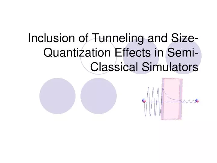
Inclusion of Tunneling and Size-Quantization Effects in Semi-Classical Simulators
Outline: • What is Computational Electronics? • Semi-Classical Transport Theory • Drift-Diffusion Simulations • Hydrodynamic Simulations • Particle-Based Device Simulations • Inclusion of Tunneling and Size-Quantization Effects in Semi-Classical Simulators • Tunneling Effect: WKB Approximation and Transfer Matrix Approach • Quantum-Mechanical Size Quantization Effect • Drift-Diffusion and Hydrodynamics: Quantum Correction and Quantum Moment Methods • Particle-Based Device Simulations: Effective Potential Approach • Quantum Transport • Direct Solution of the Schrodinger Equation (Usuki Method) and Theoretical Basis of the Green’s Functions Approach (NEGF) • NEGF: Recursive Green’s Function Technique and CBR Approach • Atomistic Simulations – The Future • Prologue
Quantum Mechanical Effects There are three important manifestations of quantum mechanical effects in nano-scale devices: - Tunneling - Size Quantization - Quantum Interference Effects
Inclusion of Tunneling and Size-Quantization Effects • Tunneling Effect: WKB Approximation and Transfer Matrix Approach • Quantum-Mechanical Size Quantization Effect • Drift-Diffusion and Hydrodynamics: • Quantum Correction and • Quantum Moment Methods • Particle-Based Device Simulations: Effective Potential Approach
Tunneling Currents vs. Technology Nodes and Tunneling Mechanisms This slide is courtesy of D. K. Schroder.
WKB Approximation to Tunneling Currents Calculation - eEx FB FB EF EF a x-axis 0 0 No applied bias With applied bias • The difference between the Fermi level and the top of the barrier is denoted by FB • According to WKB approximation, the tunneling coefficient through this triangular barrier equals to: where:
WKB Approximation to Tunneling Currents Calculation • The final expression for the Fowler-Nordheim tunneling coefficient is: • Important notes: • The above expression explains tunneling process only qualitatively because the additional attraction of the electron back to the plate is not included • Due to surface imperfections, the surface field changes and can make large difference in the results Calculated and experimental tunnel current characteristics for ultra-thin oxide layers. (M. Depas et al., Solid State Electronics, Vol. 38, No. 8, pp. 1465-1471, 1995)
Tunneling Current Calculation in Particle-Based Device Simulators • If the device has a Schottky gate then one must calculate both the thermionic emission and the tunneling current through the gate • WKB fails to account for quantum-mechanical reflections over the barrier • Better approach to use in conjunction with particle-based device simulations is the Transfer Matrix Approach W. R. Frensley, “Heterostructure and Quantum Well Physics,” ch. 1 in Heterostructure and Quantum Devices, a volume of VLSI Electronics: Microstructure Science, N. G. Einspruch and W. R. Frensley, eds., (Academic Press, San Diego, 1994).
Transfer Matrix Approach Within the Transfer Matrix approach one can assume to have either • Piece-wise constant potential barrier • Piecewise-linear potential barrier D. K. Ferry, Quantum Mechanics for Electrical Engineers, Prentice Hall, 2000.
Piece-Wise Constant Potential Barrier (PCPBT Tool) installed on the nanoHUB www.nanoHUB.org
The Approach at a Glance Slide property of Sozolenko.
The Approach, Continued Slide property of Sozolenko.
Piece-Wise Linear Potential Barrier • This algorithm is implemented in ASU’s code for modeling Schottky junction transistors (SJT) • It approximates real barrier with piece-wise linear segments for which the solution of the 1D Schrodinger equation leads to Airy functions and modified Airy functions • Transfer matrix approach is used to calculate the energy-dependent transmission coefficient • Based on the value of the energy of the particle E, T(E) is looked up and a random number is generated. If r<T(E) than the tunneling process is allowed, otherwise it is rejected. Tarik Khan, PhD Thesis, December 2004.
1D Schrödinger equation: Solution for piecewise linear potential: The total transmission matrix: T(E): Vi+1 Vi E Vi-1 V(x) ai-1 ai ai+1 The Approach at a Glance
Simulation Results for Gate Leakage in SJT T. Khan, D. Vasileska and T. J. Thornton, “Quantum-mechanical tunneling phenomena in metal-semiconductor junctions”, NPMS 6-SIMD 4, November 30-December 5, 2003, Wailea Marriot Resort, Maui, Hawaii.
Quantum-Mechanical Size Quantization Quantum-mechanical size quantization manifests itself as: - Effective charge set-back from the interface - Band-gap increase - Modification of the Density of States function D. Vasileska, D. K. Schroder and D.K. Ferry, “Scaled silicon MOSFET’s: Part II - Degradation of the total gate capacitance”, IEEE Trans. Electron Devices 44, 584-7 (1997).
Gate Substrate Effective Charge Set-Back From The Interface • Schrodinger-Poisson Solvers • Quantum Correction Models • Quantum Moment Models D. Vasileska, and D.K. Ferry, "The influence of poly-silicon gates on the threshold voltage, inversion layer and total gate capacitance in scaled Si-MOSFETs," Nanotechnology Vol. 10, pp.192-197 (1999).
Schrödinger-Poisson Solvers • At ASU we have developed: • 1D Schrodinger – Poisson Solvers (inversion layers and heterointerfaces) • 2D Schrodinger – Poisson solvers (Si nanowires) • 3D Schrodinger – Poisson solvers (Si quantum dots) S. N. Miličić, F. Badrieh, D. Vasileska, A. Gunther, and S. M. Goodnick, "3D Modeling of Silicon Quantum Dots," Superlattices and Microstructures, Vol. 27, No. 5/6, pp. 377-382 (2000).
Space Quantization Literature Bacarani and Worderman transconductance degradation (Proceedings of the IEDM, pp. 278-281, 1982) Hartstein and Albert estimate of the inversion layer thickness (Phys. Rev. B, Vol. 38, pp.1235-1240, 1988) van Dort et al. analytical model for Vth which accounts for QM effects (IEEE TED, Vol. 39, pp. 932-938, 1992) Takagi and Toriumi physical origins of Cinv (IEEE TED, Vol. 42, pp. 2125-2130, 1995) Vasileska, Schroder and Ferry influence of many-body effects on Cinv (IEEE TED, Vol. 44, pp. 584-587, 1997) Hareland et al. modeling of the QM effects in the channel (IEEE TED, Vol. 43, pp. 90-96, 1996) Krisch et al. poly-gate capacitance attenuation (IEEE EDL, Vol. 17, pp. 521-524, 1996)
1D Schrodinger-Poisson Solver for Si Inversion Layers – SCHRED
Simulation Results Obtained With SCHRED • The classical charge density peaks right at the SC/oxide interface. • The quantum-mechanically calculated charge density peaks at a finite distance from the SC/oxide interface, which leads to larger average displacement of electrons from that interface. • Cinv reduces Ctot by about 10% • Cpoly+ Cinv reduce Ctot by about 20% • With poly-depletion Ctot has pronoun-ced gate-voltage dependence
Simulation Results Obtained With SCHRED Degradation of the Total Gate Capacitance Ctot for Different Device Technologies
Comparison With Experiments D. Vasileska, PhD Thesis, 1995.
SCHRED Usage on the nanoHUB • SCHRED has 92 citations in Scientific Research Papers, 1481 users and 36916 jobs as of July 2009
3D Schrodinger-Poisson Solvers • 3D Schrodinger – ARPACK • 3D Poisson: BiCGSTAB method
3D Schrodinger-Poisson Solvers Left: The energy level spacing distribution as a function of s =DE/(DE)avg obtained by combining the results of a number of impurity configurations. Right: The 11th to 16th eigenstates of the silicon quantum dot. S. N. Milicic, D. Vasileska, R. Akis, A. Gunther, and S. M Goodnick, "Discrete impurity effects in silicon quantum dots," Proceedings of the 3rd International Conference on Modeling and Simulation of Microsystems, San Diego, California, March 27-29, 2000, pp. 520-523 (Computational Publications, 2000).
Modification of the DOS Function • The modification of the DOS function affects the scattering rates and must be accounted for in the adiabatic approximation via solution of the 1D/2D Schrodinger equation in slices along the channel of the device • This is time consuming and for all practical purposes only charge set-back and modification of the band-gap are to a very good accuracy accounted for using either • Bohm potential approach to continuum modeling • Effective potential approach in conjunction with particle-based device simulators
Quantum Corrected Approaches Drift Diffusion Density Gradient Hydrodynamic Quantum Hydrodynamic Particle-based device simulations Effective Potential Approaches due to: - Ferry, and - Ringhofer and Vasileska
D. Vasileska and S. S. Ahmed, “Modeling of Narrow-Width SOI Devices”, Semicond. Sci. Technol., Vol. 19, pp. S131-S133 (2004). D. Vasileska and S. S. Ahmed, “Narrow-Width SOI Devices: The Role of Quantum Mechanical Size Quantization Effect and the Unintentional Doping on the Device Operation”, IEEE Transactions on Electron Devices, Volume 52, Issue 2, Feb. 2005 Page(s):227 – 236.
Summary • Tunneling that utilizes transfer matrix approach can quite accurately be included in conjunction with particle-based device simulators • Quantum-mechanical size-quantization effect can be accounted in fluid models via quantum potential that is proportional to the second derivative of the log of the density • Effective potential approach has been proven to include size-quantization effects rather accurately in conjunction with particle-based device simulators • Neither the Bohm potential nor the effective potential can account for the modification of the density of states function, and, therefore, scattering rates modification because of the low-dimensionality of the system, and, therefore, mobility and drift velocity