1 / 34

Table 8.1 Verilog 2001 HDL Operators

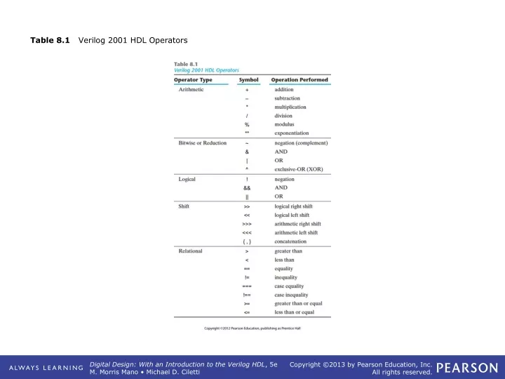
Table 8.1 Verilog 2001 HDL Operators. Table 8.2 Verilog Operator Precedence. FIGURE 8.1 A simplified flowchart for HDL‐based modeling, verification, and synthesis. FIGURE 8.2 Control and datapath interaction. FIGURE 8.3 ASM chart state box. FIGURE 8.4 ASM chart decision box.

sellers
Download Presentation

Table 8.1 Verilog 2001 HDL Operators

An Image/Link below is provided (as is) to download presentation Download Policy: Content on the Website is provided to you AS IS for your information and personal use and may not be sold / licensed / shared on other websites without getting consent from its author. Content is provided to you AS IS for your information and personal use only. Download presentation by click this link. While downloading, if for some reason you are not able to download a presentation, the publisher may have deleted the file from their server. During download, if you can't get a presentation, the file might be deleted by the publisher.

E N D

Presentation Transcript


  1. Table 8.1 Verilog 2001 HDL Operators

  2. Table 8.2 Verilog Operator Precedence

  3. FIGURE 8.1 A simplified flowchart for HDL‐based modeling, verification, and synthesis

  4. FIGURE 8.2 Control and datapath interaction

  5. FIGURE 8.3 ASM chart state box

  6. FIGURE 8.4 ASM chart decision box

  7. FIGURE 8.5 ASM chart conditional box and examples

  8. FIGURE 8.6 ASM blocks

  9. FIGURE 8.7 State diagram equivalent to the ASM chart of Fig. 8.6

  10. FIGURE 8.8 Transition between states

  11. FIGURE 8.9 (a) Block diagram for design example (b) ASMD chart for controller state transitions, asynchronous reset (c) ASMD chart for controller state transitions, synchronous reset (d) ASMD chart for a completely specified controller, asynchronous reset

  12. Table 8.3 Sequence of Operations for Design Example

  13. FIGURE 8.10 Datapath and controller for design example

  14. FIGURE 8.11 Register transfer‐level description of design example

  15. Table 8.4 State Table for the Controller of Fig. 8.10

  16. FIGURE 8.12 Logic diagram of the control unit for Fig. 8.10

  17. FIGURE 8.13 Simulation results for Design_Example_RTL

  18. FIGURE 8.14 (a) Block diagram and (b) datapath of a binary multiplier

  19. FIGURE 8.15 ASMD chart for binary multiplier

  20. Table 8.5 Numerical Example For Binary Multiplier

  21. FIGURE 8.16 Control specifications for binary multiplier

  22. Table 8.6 State Assignment for Control

  23. Table 8.7 State Table for Control Circuit

  24. FIGURE 8.17 Logic diagram of control for binary multiplier using a sequence register and decoder

  25. FIGURE 8.18 Logic diagram for one‐hot state controller

  26. FIGURE 8.19 Simulation waveforms for one‐hot state controller

  27. FIGURE 8.20 Example of ASM chart with four control inputs

  28. FIGURE 8.21 Control implementation with multiplexers

  29. Table 8.8 Multiplexer Input Conditions

  30. FIGURE 8.22 Block diagram and ASMD chart for count‐of‐ones circuit

  31. Table 8.9 Multiplexer Input Conditions for Design Example

  32. FIGURE 8.23 Control implementation for count‐of‐ones circuit

  33. FIGURE 8.24 Simulation waveforms for count‐of‐ones circuit

  34. FIGURE 8.24 (continued) Simulation waveforms for count‐of‐ones circuit

More Related