Download
1 / 2
30 likes | 293 Views
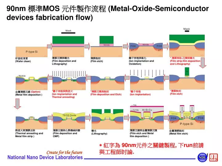
90nm 標準 MOS 元件製作流程 (Metal-Oxide-Semiconductor devices fabrication flow). 薄膜沉積與曝光 (Film deposition and Lithography). 離子佈植與氧化 (Ion implantation and Oxidation).

E N D
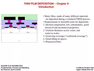
90nm 標準MOS 元件製作流程 (Metal-Oxide-Semiconductor devices fabrication flow) 薄膜沉積與曝光 (Film deposition and Lithography) 離子佈植與氧化 (Ion implantation and Oxidation) * 薄膜移除,沉積與曝光 (Film strip;film deposition and Lithography) 薄膜蝕刻 (Film etch) 矽基板清潔 (Wafer clean) *薄膜蝕刻 (Film etch) *離子佈植與熱退火 (Ion implantation and Thermal annealing) *薄膜沉積與蝕刻 (Film deposition and Etch) *離子佈植 (Ion implantation) 金屬薄膜沉績 (Option) (Metal film deposition ) 熱退火與薄膜去除 (Thermal annealing and Metal film strip ) 薄膜沉積與化學機械研磨 (Film deposition and CMP) 薄膜沉績與金屬薄膜沉積(Film etch and Metal film deposition) 曝光 (Lithography) 金屬薄膜蝕刻 (Metal film etch) 紅字為 90nm元件之關鍵製程, 下run前請與工程師討論.