Download
1 / 16
170 likes | 381 Views
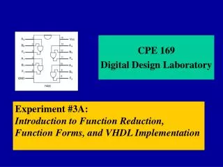
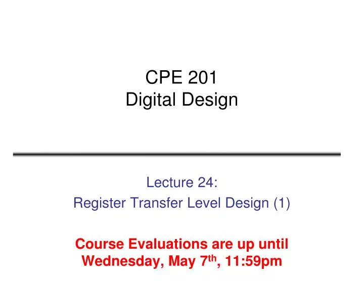
CPE 201 Digital Design. Lecture 24: Register Transfer Level Design (1) Course Evaluations are up until Wednesday, May 7 th , 11:59pm. Lecture Outline. RTL Design Datapath Control. bi. bo. FSM outputs. FSM inputs. Combinational logic. n1. n0. s1. s0. State register. clk.

E N D
CPE 201Digital Design Lecture 24: Register Transfer Level Design (1) Course Evaluations are up until Wednesday, May 7th, 11:59pm
Lecture Outline • RTL Design • Datapath • Control
bi bo FSM outputs FSM inputs Combinational logic n1 n0 s1 s0 State register clk Register Transfer Level – Introduction • Controllers • Control input/output: single bit (or just a few) representing an event • Finite-state machine describes behavior; implemented as state register and combinational logic • Datapath components • Data input/output: Multiple bits collectively representing single entity • Datapath components include registers, adders, comparators, register files, etc. Register Comparator Register file
bi bo Combinational logic n1 n0 s1 s0 State register Register Transfer Level – Introduction • Custom processors • Controller and datapath components working together to implement an algorithm • Examples • Noise filter for audio signal, data encryption, fingerprint identification, image processing Register file Datapath Controller
RTL Design: Capture Behavior, Convert to Circuit • Combinational Logic Design • First step: Capture behavior (using equation or truth table) • Remaining steps: Convert to circuit • Sequential Logic Design • First step: Capture behavior (using FSM) • Remaining steps: Convert to circuit • RTL Design (the method for creating custom processors) • First step: Capture behavior (using high-level state machine, to be introduced) • Remaining steps: Convert to circuit Capture behavior Convert to circuit
RTL System Design • A system is represented at Register Transfer Level when it is specified by the following: • Set of registers in the system • Operations performed on data stored in registers • Control that supervises the sequences of operations • Registers • Load, shift, counters • Operations • Replace information in register, transfer to another register • Control • Timing signals that sequence the operations in a prescribed manner
Operations with Registers • Information transfer • R2 R1 • Conditional transfer • If (T1 = 1) then (R2 R1) (T1- control signal) • Multiple operations • If (T3 = 1) then (R2 R1, R4 R3) • Other examples • R1 R1 + R2 (addition) • R3 R3 + 1 (increment by 1) • R4 shr R4 (shift right R4) • R5 0 (clear R5) Parallel adder, registers Counter Shift register Register w/ clear input
Register file Datapath Controller bi bo Combinational logic n1 n0 s1 s0 State register Control & Datapath Interaction • Datapath • Manipulates data in registers, according to requirements • Controller • Uses status conditions from datpath to determine control sequence • Higher-level state machine
25 s s a a 25 50 1 1 0 0 c c Soda Soda d d dispenser dispenser 0 0 processor processor RTL Design Method: “Preview” Example • Soda dispenser • c: bit input, 1 when coin deposited • a: 8-bit input having value of deposited coin • s: 8-bit input having cost of a soda • d: bit output, processor sets to 1 when total value of deposited coins equals or exceeds cost of a soda 0 tot: 50 tot: 25 1 How can we precisely describe this processor’s behavior?
s a 8 8 c Soda d dispenser processor c Add I nit Wait tot=tot+a c’*(tot<s) d=0 c’*(tot<s)’ tot=0 Disp d=1 Preview Example: Step 1 Capture High-Level State Machine • Declare local register tot • Init state: Set d=0, tot=0 • Wait state: wait for coin • If see coin, go to Add state • Add state: Update total value: tot = tot + a • Remember, a is present coin’s value • Go back to Wait state • In Wait state, if tot >= s, go to Disp(ense) state • Disp state: Set d=1 (dispense soda) • Return to Init state Inputs: c (bit), a (8 bits), s (8 bits) Outputs: d (bit) Local registers: tot (8 bits)
I nputs : c (bit), a(8 bits) , s (8 bits) O utputs : d (bit) L ocal r e g is t ers : t ot (8 bits) s a c A dd I nit W ait t ot= t ot+a * tot_ld ‘ c ( t ot<s) ld d=0 c ‘ ( tot ‘ t ot<s) t ot=0 tot_clr clr Disp 8 d=1 8 8 8-bit 8-bit tot_lt_s adder < 8 Datapath Preview Example: Step 2 Create Datapath • Need tot register • Need 8-bit comparator to compare s and tot • Need 8-bit adder to perform tot = tot + a • Wire the components as needed for above operations • Create control input/outputs, give them names
s a t ot_ld ld t ot t ot_clr clr 8 8 8 8-bit 8-bit t ot_lt_s adder < 8 D a tap a th Preview Example: Step 3 Connect Datapath to a Controller • Controller’s inputs • External input c (coin detected) • Input from datapath comparator’s output, which we named tot_lt_s • Controller’s outputs • External output d (dispense soda) • Outputs to datapath to load and clear the tot register s a 8 8 c d tot_ld tot_clr Controller Datapath tot_lt_s
I nputs : c (bit), a(8 bits) , s (8 bits) O utputs : d (bit) L ocal r e g is t ers : t ot (8 bits) c A dd I nit W ait s a t ot= t ot+a * ‘ c ( t ot<s) d=0 c ‘ ( tot_lt_s’ ‘ t c’* ot<s) t ot=0 tot_ld ld Disp tpt tot_clr clr Inputs: c , tot_lt_s (bit) Outputs: d , tot_ld , tot_clr (bit) d=1 8 tot_ld 8 8 c c Add tot_clr tot_lt_s d 8-bit I nit W ait 8-bit tot_ld=1 tot_lt_s adder < * c ’ tot_lt_s d=0 8 tot_clr=1 Datapath Disp d=1 Controller Preview Example: Step 4 Derive the Controller’s FSM s a • Same states and arcs as high-level state machine • But set/read datapath control signals for all datapath operations and conditions 8 8 c d tot_ld tot_clr Datapath Controller tot_lt_s
Inputs: c , tot_lt_s (bit) Outputs: d , tot_ld , tot_clr (bit) tot_lt_s’ c’* tot_ld c c Add tot_clr d I nit W ait tot_ld=1 tot_lt_s * c ’ tot_lt_s d=0 tot_clr=1 Disp d=1 Controller Preview Example: Completing the Design • Implement the FSM as a state register and logic • Table shown on right
Readings • Chapter 8 • Sections 8.1-8.4