Download
1 / 16
170 likes | 572 Views
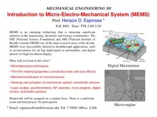
Micromirror Lithography. David Chen EECS 277. Overview. What is Lithography? What are Micromirrors? Successful Research Future. What is Lithography?. It is the backbone of nearly all semiconductor device fabrication processes. It allows for high precision and tiny devices.

E N D
Micromirror Lithography David Chen EECS 277
Overview • What is Lithography? • What are Micromirrors? • Successful Research • Future
What is Lithography? • It is the backbone of nearly all semiconductor device fabrication processes. • It allows for high precision and tiny devices. • It allows for mass production. • For the most part, it removes human error from the manufacturing process, giving high yield production.
What is Lithography? The procedure for lithography is as follows: • Start with a wafer • Deposit or grow layer of desired material • Spin coat photoresist • Pattern photoresist by exposure • Etch layer underneath or deposit/grow new layer • Remove photoresist • Repeat
What is Photoresist? • Light sensitive material • Changes molecular bond after exposure to certain wavelengths of light • Used to make planar patterns determined by photomasks • Protects layers underneath during etching • Can be easily removed after each process
Example of Lithography • A familiar device: CMOS inverter • Link • 7 different photoresist patterns • 7 different photomasks • Very simple device
Masks Cost How Much?!? • Costs per mask-set • 65nm ~ $1million • 45nm ~ $2.2million • 32nm ~ $4million • 28nm ~ $8million • Bearable for high volume manufacturers • Outrageous for small companies or prototyping • Masks also deteriorate after use!
Why are masks so expensive? • Very high resolution structures require expensive processes such as electron beam etching or laser etching (also lithography) • Unique pattern means masks are custom made per client order • Need an alternative • What other things produce high resolution images… • AKA high definition images… • AKA HD…
We Already Have the Technology! • Made famous by Texas Instrument’s DLP (digital light processing) televisions • DMD- digital micromirror device • Project high resolution images
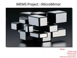
What Are Micromirrors? • MEMS (Micro-electro-mechanical systems) • Array of millions of mirrors on a tiny chip • Each mirror can be independently controlled • On/Off states
TV vs. Maskless Lithography • Even though they’re HD, TV pixels are still way too big for lithography • We are trying to pattern photoresist on the sub-micron scale! • Need a HUGE lens to focus the array to a smaller scale • Making a huge lens is hard.
One Solution from MIT: ZPAL • Using an equal number of array of diffracting lenses fabricated by lithography, each beam of light can be focused individually. • Feature sizes can be much smaller than the beam width!
Results from test • Well defined structures • Low roughness • Features on spot size scale • Done using UV light
Future Improvements • Smaller wavelength light • EUV (extreme UV) 120nm-10nm • X-Ray 10nm-1pm • Higher refractive mediums • Liquid immersed fabrication • = Smaller spot size
Benefits of Micromirror Lithography • Programmable “mask” • Vs. permanent photomask • No cost for prototype masks • Vs. $millions per set • Instant mask production • Vs. weeks to months per set • All of the above = Cheaper!
Resources • http://www.eetimes.com/showArticle.jhtml;jsessionid=ONC4WJBQYCVL0QSNDLRSKHSCJUNN2JVN?articleID=211100224 • http://jas.eng.buffalo.edu/education/fab/invFab/index.html • http://www.eetimes.com/showArticle.jhtml;jsessionid=ONC4WJBQYCVL0QSNDLRSKHSCJUNN2JVN?articleID=211100224 • http://nanoweb.mit.edu/zpal/Presentations/SPIE_2005_web.pdf • http://nanoweb.mit.edu/zpal/Presentations/EIPBN-2004-Alpha.pdf • http://nanoweb.mit.edu/zpal/Presentations.html • http://nanoweb.mit.edu/zpal/Presentations/EIPBN-2004-SSP.pdf