Download
1 / 1
20 likes | 203 Views
Self Forming Barrier Layers from CuX Thin Films . Project Background. CuX Resistivity Study (X= Ge , Ni, Mn , Ti). Shamon Walker, Erick Nefcy , Samir Mehio. Ultra thin diffusion barriers (between Cu and SiO 2 ) are required for super computing. .

E N D
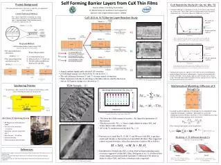
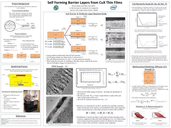
Self Forming Barrier Layers from CuX Thin Films Project Background CuX Resistivity Study (X= Ge, Ni, Mn, Ti) Shamon Walker, Erick Nefcy, SamirMehio • Ultra thin diffusion barriers (between Cu and SiO2) are required for super computing. • CuTi and CuMn have a minimum resistivity of 6.9 μΩ-cm and 3.02μΩ-cm, respectively. These values, however, did not quite satisfy the project requirements of < 3.0 μΩ-cm . However, CuMn was very close. Dr. Milo Koretsky, Eric Gunderson, Kurt Langworthy Sponsors: Intel, Oregon Metals Initiative , ONAMI Current Industrial Method: • The current deposition orientation for laying interconnect material on an integrated circuit uses a tantalum nitride (TaN)/tantalum barrier to keep SiO2 separate from Cu: • Si/SiO2/TaN/Ta/Cu. CuTi (5.6 at. % Ti) Barrier Layer Reaction Study Pre-anneal air exposure No pre-anneal air exposure CuTi A1 Possible Oxide Barrier Layer SiO2 Figure 7. A plot showing the affect of anneal time on thin film resistivity of CuMn. One group of samples was exposed to air before annealing and the other was not exposed to air before annealing. All films were 7 at. % X and annealed at 500oC in Ar at 30 mTorr.. Figure 1. Scanning Electron Microscope (SEM) image of a CuTi (5.6 at.% Ti) alloy annealed for 2 hrs at 500oC in O2. Proposed Method: • Self forming barrier layers using CuX • (where X = Mg, Mn, Ge, Ni, Ti, and Al) CuTi Pre-anneal air exposure B1 • Pre-anneal deposition orientation: • Si/SiO2/CuX • Post-anneal deposition orientation may be: • Si/SiO2/Metal Oxide/Cu Possible Oxide Barrier Layer Cu7Ti2 Project Requirements: A1 SiO2 B1 4-10 nm barrier layer Film resistivity < 3.0 μΩ-cm No detectable interdiffusion between Cu and SiO2. No pre-anneal air exposure C1 Figure 2. SEM image of a CuTi (5.6 at.% Ti) alloy annealed for 2 hrs at 500oC in UHV with NO pre-anneal air exposure. Figure 8. A plot showing the affect of anneal time on thin film resistivity of CuTi. One group of samples was exposed to air before annealing and the other was not exposed to air before annealing. All films were 7 at. % X and annealed at 500oC in Ar at 30 mTorr.. CuTi C1 • Anneal ambient significantly affected CuTi structure. • A CuTi phase change was observed for B1 but not for C1. • The only difference between B1 and C1 was pre-anneal air exposure. • Water molecules from the air adsorbing to the films surface could be the reason why no CuTi phase change was observed in C1. • Prolonged pre-anneal air exposure is believed to be the reason behind the peculiar shape of the curves in both figures. Oxygen and water molecules adsorb to the films surface during exposure and eventually form a surface oxide. These ultra thin oxides are highly resistive, and increase the value of the measured resistivity (seen above). Possible Oxide Barrier Layer SiO2 Fig 3. SEM image of a CuTi (5.6 at.% Ti) alloy annealed for 2 hrs at 500oC in UHV w/ pre-anneal air exposure of 30 days. Sputtering Process TEM Sample – B1 Mathematical Modeling: Diffusion of X through Cu • In sputtering, a film is grown by the ejection of material from a solid surface following the impact of energetic ions. SiO2 Barrier Layers CuTi • A simple model for diffusion of X through Cu was formulated using symmetrical boundary conditions. The model was created by combining a material balance and Fick’s 1st law of Diffusion for a thin slab. The governing equation can be seen below: Figure 6. A plot of the Gibbs energy of reaction vs. reaction temperature for an assumed redox reaction of M + SiO2 → MxOy + Si. Pt AJA Orion IV Sputtering System • The lower the Gibbs energy of reaction…the larger the spontaneity of the reaction. • The data sets with < 0 have a high affinity to reduce SiO2 and form a metal oxide of their own. • All of the Ti oxidation reactions have < 0. • RF Magnetron 300W dual power supply • Two mass-flow controllers (Ar and O2) • Maximum substrate temperature: • 850oC • Base Pressure ≈ 1E-08 Torr • Substrate Rotation • Three magnetron sputtering guns Figure 4. Transmission Electron Microscope (TEM) image of a CuTi (5.6 at.% Ti) alloy annealed for 2 hrs at 500oC in UHV with NO pre-anneal air exposure. • The solution to the model can be found below: SiO2 • Pretorius et al. found that Ti, Zr, Hf, V, and Nb react with SiO2 to produce oxides and silicides at the interfaces of metal/SiO2/Si films. They suggested a direct reaction between a silica film and metal overlayer (M) as follows: Modeling of Ti diffusion through Cu • CuTi (5.6 at. % Ti) annealed at 500oC TixSi TiyO2 Center Profile Center of Film • References • Qiang Fu, Thomas Wagner, Interaction of nanostructured metal overlayers with oxide surfaces, Surf. Sci. 62 (2007) 431-498 • R. Pretorius, J.M. Harris, M.A. Nicolet, Reaction of thin metal films with SiO2 substrates, Solid State Electron. 21 (1978) • H. Dallaporta, M. Liehr, J.E. Lewis, Silicon dioxide defects induced by metal impurities, Phys. Rev. B 41 (1990) 5075 CuTi • Interdiffusion of metals into SiO2 is often observed upon annealing metal overlayers supported on thin SiO2 films (Dallaporta et al.). It is believed that a large chemical potential gradient facilitates Ti diffusion to the interface where it reduces SiO2 and forms a titanium oxide compound. Edge Profile Figure 9. Plot of Ti concentration in Cu as a function of anneal time and distance from each edge in a 430nm CuTi film. Figure 10. Plot of Ti concentration in Cu as a function of anneal time and distance from each edge in a 430nm CuTi film. Figure 5. TEM image of CuTi/SiO2 interface. The CuTi (5.6 at. % Ti) film was annealed for 2 hrs at 500oC in UHV with NO pre-anneal air exposure.