Download
1 / 45
460 likes | 577 Views
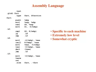
MCS51 ASSEMBLY Language. Resources http://atmel.com/dyn/products/. Pin configuration. Block Diagram. Memory addresses. with 5 address spaces Program memory/Code address space up to 64 K bytes Data Memory Directly addressable Normally 128 bytes low address (0-07FH)

E N D
MCS51 ASSEMBLY Language Resources http://atmel.com/dyn/products/ CIT 673 Created by Suriyong
Pin configuration CIT 673 Created by Suriyong
Block Diagram CIT 673 Created by Suriyong
Memory addresses • with 5 address spaces • Program memory/Code address space up to 64 K bytes • Data Memory • Directly addressable • Normally 128 bytes low address (0-07FH) • Expand to 256 bytes depend on CPU type (0-0FFH) • Indirectly addressable • for address 0-0x7f is the same page of direct address • for 0x80-0xff is the another page • External data address – up to 64K • Bit address space • same location to data memory address 0x20 – 0x2F • 16 bytes: 128 bit address (0x00 – 0x7f) CIT 673 Created by Suriyong
Program memory address space • 2 configuration controlled by /EA pin (External Address) Internal + external EA = “1” External Only EA = “0” CIT 673 Created by Suriyong
255 127 47 31 HARDWARE REGISTER MAPPING NOT AVAILABLE FOR THE 8031 ON-CHIP RAM DIRECTLY/INDIRECTLY ADDRESSABLE ON-CHIP RAM RAM BIT ADDRESS SPACE 4 REGISTER BANKS 7 0 Data Memory Internal data memory allocation CIT 673 Created by Suriyong
Direct addressing area • 2 pages : 128 bytes each • lower area : 0x00-0x7f • general purpose • address 0x20 – 0x2F is bit addressable • able to use both direct and indirect addressing mode • higher area : 0x80 – 0xff with 2 pages • 1st page is conserved for SFR (Special Function Register) area • use direct addressing mode • 2nd page is general purpose, access with indirect addressing CIT 673 Created by Suriyong
Basic internal data memory extra page of internal memory for other version of MCS51 (8052 etc): use indirect addressing mode CIT 673 Created by Suriyong
External data memory • MCS51 able to expand the data memory called external data memory • up to 64K bytes • use both direct and indirect addressing mode • not prefer when CPU operate in 1 chip mode CIT 673 Created by Suriyong
External data memory configuration AT89S8252 PROGRAM MEMORY CONFIGURATION EXTERNAL DATA MEMORY CONFIGURATION MCS51 data memory, the external and internal are independent CIT 673 Created by Suriyong
Bit addressable layout CIT 673 Created by Suriyong
The Registers • locate at 0x80 – 0xff address except register R0-R7 at 4 banks of lower address 0x00 – 0x1f • 2 type of register • General Purpose registers • Auxiliary/ Accumulator register (Acc or A) • Multiplication/Scratch Pad Register (B) • Stack pointer (SP) • Data Pointer DPH/DPL -> DPTR • Program Status Word – PSW • Special Function Registers • SBUF, SCON…TMOD • Interrupt Enable/Priority (IE/ IP) • Port register P0,P1,P2 and P3 • etc. • Both type bit addressable or not depend on register duty • see more detail for each register CIT 673 Created by Suriyong
Register layout No name box is empty and conserve for future version CIT 673 Created by Suriyong
Register layout bit addressable display CIT 673 Created by Suriyong
General Purpose registers • 8 registers with 4 banks 8 bytes/bank • R0-R7 • location 00H-1FH • 4 banks selection controlled by RS0,RS1 bit in PSW • often used in couple such as R0:R2, R1:R3 formed as 16 bit register CIT 673 Created by Suriyong
Stack Pointer (SP) • initialize set to RAM location 07H • Last In First Out (LIFO) mechanism • store Program Counter, PSW etc. • not exceed 127 • increment when use CIT 673 Created by Suriyong
PSW – Program Status Word • For operation checking or status such as carry flag, overflow flag Status for ALU operation CIT 673 Created by Suriyong
The SFR • Port: P0 – P3 perform 32 bit addressable independent I/O port • Timer/Counter : T0 – T2 • 8 bit, timer/counter with internal/external input • SBUF, SCON • Serial communication buffer and control • etc. CIT 673 Created by Suriyong
Instruction group of MCS51 assembly language • Operation • Arithmetic • logical • boolean • Data transfer • Program control CIT 673 Created by Suriyong
Arithmetic operation • Effect PSW register • OV, CY and AC flag • Command set • ADD, ADDC : ADD, with Carry • SUB, SUBB : SUBtract, with Borrow • MUL : Register Multiplication • DIV : Register Division • INC : Increment • DEC : Decrement • DAA : Decimal Adjust • example • ADDC A, #07FH ; add register a with 07f and carry and ; store in A • Question: Show the event that effect OV, CY and AC CIT 673 Created by Suriyong
Logical Operation • ANL : AND with accumulator • ORL : logical OR with accumulator • XRL : logical XOR with accumulator • CLR : CLeaR accumulator to zero • CPL : Complement • RL, RLC : Rotate Left, with Carry flag • RR, RRC : Rotate Right, with Carry flag • SWAP : Swap nibble within accumulator CIT 673 Created by Suriyong
Boolean Manipulation • manipulate bit or flag • use Carry flag as bit accumulator • CLR C, bit; clear carry or bit • SETB C or bit; set carry or bit to “1” • CPL C or bit, bit complement • ANL C, bit; C=C and bit • ORL • MOV C, bit; move with carry CIT 673 Created by Suriyong
Data transfer • MOV A, <source> ; copy with Accumulator • MOVC A, <indirect>; move code with acc • MOVX A, <indirect>; move external with ; acc • PUSH & POP ; push and pop to stack • XCH A, <source> ; exchange with acc • XCHD A, Rn ; exchange register with A, ; low nibble digit CIT 673 Created by Suriyong
Machine control • Jump • with condition • JZ/JNZ ; Jump if Zero flag/non zero flag • JC/JNC ; Jump if carry flag/non carry flag • JB/JNB direct; Jump if direct bit/not direct bit • CJNE ; compare jump if not equal • DJNZ; Decrement and Jump if non zero • no condition • AJUP/LJMP/SJMP • JMP @A+DPTR ; jump indirect • CALL • ACALL, LCALL with 11bit, 16 bit address • Return • RET ; return • RETI ; return from interrupt • NOP ; no operation CIT 673 Created by Suriyong
The addressing mode • Register addressing • source can be either register R0 – R7 • MOV A, R0 • Direct addressing • Source is represented with memory location • MOV A, 07FH • Indirect • source is register and its content is index point to the data location • source is used together with “@” sign • MOV A, @R0; copy to A with the content of R0 point to • Immediate • source is numeric value • precede with “#” sign • MOV A, #07FH CIT 673 Created by Suriyong
Indirect Addressing • register contain the address of memory instead • normally affect the on-chip RAM • use at sign “@” in the instruction • example • MOV A, @Rn • MOV @Rn, #07fh CIT 673 Created by Suriyong
Bit Addressing • affect the bit addressable area • may name or define the bit address • eg. SETB TR1 ; set bit Timer reset of Timer1 • SETB 88H.6 ; set the bit at address 88H bit 6 CIT 673 Created by Suriyong
For external data memory • Indirect access only • Use with data transfer instruction group • add C for Code, X for external data memory to the operation • Use register DPTR (DPH:DPL) for point to either code and data • example • MOVX A, @DPTR; • MOVX A, @A+DPTR; • move the content the dptr is point to register A • MOVC A, @A+DPTR CIT 673 Created by Suriyong
Instruction Summary • MOV Rn,#data Move immediate data to register • MOV direct,A Move Accumulator to direct byte • MOV direct,Rn Move register to direct byte • MOV direct,direct Move direct byte to direct • MOV direct,@Ri Move indirect RAM to direct byte • MOV direct,#data Move immediate data to direct byte • MOV @Ri,A Move Accumulator to indirect RAM • MOV @Ri,direct Move direct byte to indirect RAM • MOV @Ri,#data Move immediate data to indirect RAM • MOV DPTR,#data16 Load Data Pointer with a 16-bit constant • MOVC A,@A+DPTR Move Code byte relative to DPTR to Acc • MOVC A,@A+PC Move Code byte relative to PC to Acc • MOVX A,@Ri Move External RAM (8-bit addr) to Acc • MOVX A,@DPTR Move External RAM (16-bit addr) to Acc • MOVX @Ri,A Move Acc to External RAM (8-bit addr) • MOVX @DPTR,A Move Acc to External RAM (16-bit addr) • PUSH direct Push direct byte onto stack • POP direct Pop direct byte from stack • XCH A,Rn Exchange register with Accumulator • XCH A,direct Exchange direct byte with Accumulator • XCH A,@Ri Exchange indirect RAM with Accumulator • XCHD A,@Ri Exchange low-order Digit indirect RAM with Acc • BOOLEAN VARIABLE MANIPULATION • CLR C Clear Carry • CLR bit Clear direct bit • SETB C Set Carry • SETB bit Set direct bit • CPL C Complement Carry • CPL bit Complement direct bit • ANL C,bit AND direct bit to CARRY • ANL C,/bit AND complement of direct bit to Carry • ORL C,bit OR direct bit to Carry • ORL C,/bit OR complement of direct bit to Carry • MOV C,bit Move direct bit to Carry • MOV bit,C Move Carry to direct bit • JC rel Jump if Carry is set • JNC rel Jump if Carry not set • JB bit,rel Jump if direct Bit is set • JNB bit,rel Jump if direct Bit is Not set • JBC bit,rel Jump if direct Bit is set & clear bit • PROGRAM BRANCHING • ACALL addr11 Absolute Subroutine Call • LCALL addr16 Long Subroutine Call • RET Return from Subroutine • RETI Return from interrupt • AJMP addr11 Absolute Jump • LJMP addr16 Long Jump • SJMP rel Short Jump (relative addr) • JMP @A+DPTR Jump indirect relative to the DPTR • JZ rel Jump if Accumulator is Zero • JNZ rel Jump if Accumulator is Not Zero • CJNE A,direct,rel Compare direct byte to Acc and Jump if Not Equal • CJNE A,#data,rel Compare immediate to Acc and Jump if Not Equal • CJNE Rn,#data,rel Compare immediate to register and Jump if Not Equal • CJNE @Ri,#data,rel Compare immediate to indirect and Jump if Not Equal • DJNZ Rn,rel Decrement register and Jump if Not Zero • DJNZ direct,rel Decrement direct byte and Jump if Not Zero • NOP No Operation • ARITHMETIC OPERATIONS • ADD A,Rn Add register to Accumulator • ADD A,direct Add direct byte to • ADD A,@Ri Add indirect RAM to Accumulator • ADD A,#data Add immediate data to Accumulator • ADDC A,Rn Add register to Accumulator with Carry • ADDC A,direct Add direct byte to Accumulator with Carry • ADDC A,@Ri Add indirect RAM to Accumulator with Carry • ADDC A,#data Add immediate data to Acc with Carry • SUBB A,Rn Subtract Register from Acc with borrow • SUBB A,direct Subtract direct byte from Acc with borrow • SUBB A,@Ri Subtract indirect RAM from ACC with borrow • SUBB A,#data Subtract immediate data from Acc with borrow • INC A Increment Accumulator • INC Rn Increment register • INC direct Increment direct byte • INC @Ri Increment direct RAM • DEC A Decrement Accumulator • DEC Rn Decrement Register • DEC direct Decrement direct byte • DEC @Ri Decrement indirect RAM • INC DPTR Increment Data Pointer • MUL AB Multiply A & B • DIV AB Divide A by B • DA A Decimal Adjust Accumulator • LOGICAL OPERATIONS • ANL A,Rn AND Register to Accumulator • ANL A,direct AND direct byte to Accumulator • ANL A,@Ri AND indirect RAM to Accumulator • ANL A,#data AND immediate data to Accumulator • ANL direct,A AND Accumulator to direct byte • ANL direct,#data AND immediate data to direct byte • ORL A,Rn OR register to Accumulator • ORL A,direct OR direct byte to Accumulator • ORL A,@Ri OR indirect RAM to Accumulator • ORL A,#data OR immediate data to Accumulator • ORL direct,A OR Accumulator to direct byte • ORL direct,#data OR immediate data to direct byte • XRL A,Rn Exclusive-OR register to Accumulator • XRL A,direct Exclusive-OR direct byte to Accumulator • XRL A,@Ri Exclusive-OR indirect RAM to Accumulator • XRL A,#data Exclusive-OR immediate data to Accumulator • XRL direct,A Exclusive-OR Accumulator to direct byte • XRL direct,#data Exclusive-OR immediate data to direct byte • CLR A Clear Accumulator • CPL A Complement Accumulator • RL A Rotate Accumulator Left • RLC A Rotate Accumulator Left through the Carry • RR A Rotate Accumulator Right • RRC A Rotate Accumulator Right through the Carry • SWAP A Swap nibbles within the Accumulator • DATA TRANSFER • MOV A,Rn Move register to Accumulator • MOV A,direct Move direct byte to Accumulator • MOV A,@Ri Move indirect RAM to Accumulator • MOV A,#data Move immediate data to Accumulator • MOV Rn,A Move Accumulator to register • MOV Rn,direct Move direct byte to register CIT 673 Created by Suriyong
Application with SFR • I/O PORT • TIMER/Counter • Serial communication • Interrupt control CIT 673 Created by Suriyong
Port P0 – P3 • 4 Ports, 32 bits • all bits can assign as input/output independently, • alternate function • P0: address (a0-a7) bus/data bus • P2: high address (a8-a15) bus • P3: control and i/o of Timer/counter and interrupt CIT 673 Created by Suriyong
Timer/counter • 2 timer (timer0 and time1) for standard, the same structure • SFR TCON and TMOD • container is TH:TL • 3 mode • able to use interrupt CIT 673 Created by Suriyong
Mode 0:13 bit timer/counterMode 1: 16 bit timer/counter CIT 673 Created by Suriyong
Mode 2: 8 bit auto reload CIT 673 Created by Suriyong
TMOD & TCON CIT 673 Created by Suriyong
Serial communication • MCS51 provide serial communication channel • component need • timer for communication clock (timer 1 auto reload mode) • tx : transmit channel and rx : receive channel • control register • SCON: serial control • content register • SBUF : data transmit or receive at SBUF register CIT 673 Created by Suriyong
SCON: Serial Control Register CIT 673 Created by Suriyong
Baud rate generating CIT 673 Created by Suriyong
Assembly example Two Byte Decimal Add with Registers and Constants ; BCDADD ADD THE CONSTANT 1,234 (DECIMAL) TO THE ; CONTENTS OF REGISTER PAIR (R3)(R2) ;(ALREADY A 4 BCD-DIGIT VARIABLE) ; BCDADD MOV A, R2 ADD A, #34H DA A MOV R2, A MOV A, R3 ADDC A, #12H DA A MOV R3, A RET CIT 673 Created by Suriyong
Case Statements Using CJNE CHAR EQU R7 ; CHARACTER CODE VARIABLE ; INTERP CJNE CHAR, #7FH, INTP_1 ; (SPECIAL ROUTINE FOR RUBOUT CODE) RET INTP_1 CJNE CHAR, #07H, INTP_2 ; (SPECIAL ROUTINE FOR BELL CODE) RET INTP_2 CJNE CHAR, #0AH, INTP_3 (SPECIAL ROUTINE FOR LFEED CODE) RET INTP_3 CJNE CHAR, #0DH, INTP_4 (SPECIAL ROUTINE FOR RETURN CODE) RET INTP_4 CJNE CHAR, #1BH, INP_5 (SPECIAL ROUTINE FOR ESCAPE CODE) RET INTP_5 CJNE CHAR, #20H, INTP_6 (SPECIAL ROUTINE FOR SPACE CODE) INTP_6 JC PRINTC ; JUMP IF CODE > 20H MOV CHAR, #0 ; REPLACE CONTROL CHARACTERS WITH ; NULL CODE PRINTC ; PROCESS STANDARD PRINTING CHARACTER RET CIT 673 Created by Suriyong
Implementation of Boolean function CIT 673 Created by Suriyong
Interrupt program • program that interrupt the main program • ask for service routine • 2 source of interrupt • internal such as activate by timer overflow flag • external signal source • when interrupting happen • program counter is load with corresponding address • the address contain interrupt vector point to the routine CIT 673 Created by Suriyong
concerned register CIT 673 Created by Suriyong
interrupt source and default value • default priority • IE0, TF0, IE1, TF1, RI OR TI • source address interrupt architecture CIT 673 Created by Suriyong
References • Wharton, J., An Introduction to the Intel MCS-51 Single-chip Microcontroller family, Application Notes, AP-69, May 1980, pdf document 01502a01.pdf • MCS51 microcontroller family user manual, February 1994 • 8-bit micro controller with 8 k bytes flash, Atmel 89s8252 data sheet, doc0401.pdf CIT 673 Created by Suriyong