Download
1 / 6
60 likes | 63 Views
PCB Rework Stencil: A Comprehensive Guidet<br>

E N D
For the purpose of adjusting the placement of components on an exposed PCB board, it is necessary to buy PCB rework stencil. On Printed Circuit Boards (PCBs), stencils serve two basic functions: the first is to facilitate the process of depositing solder paste, and the second is to direct a certain amount of solder paste to a particular spot on the bare PCB. The PCB stencil price does not go up due to the inclusion of the stencil’s frame, wire mesh, and steel sheet. The stencil is perforated in a number of places that correspond to specific regions of the printed circuit board. When employing a PCB Stencil to apply solder paste, the operation of assembling a PCB can be completed more quickly and successfully. Stencil Designs For PCB Boards Laser-Cut Templates Laser-cut stencils have openings sliced into them rather than etched. These lasers can be used to guarantee the holes and openings are properly aligned and exact. Chemically Etched Templates PCB stencils are printed using a destructive tool that cuts openings in metal stencils. It’s simple to assemble, but it doesn’t keep hazardous human chemicals out of the environment. Structured PCB Stencils These circuit board stencils are utilized with protective housing. A work outskirt in the housing secures the stencil sheet, allowing for precise manufacturing. Due to their high level of consistency and print quality, these stencils are employed in mass PCB manufacture. No-Frame PCB Stencils A PCB stencil that may be reused and does not require a new frame is called “frameless.” Depending on the situation, they can be placed and removed from the area in a number of different ways. They are less expensive than similar PCB stencils with outlines. There is no need for extra room if you utilize handfasting forms with frameless or reusable PCB stencils.
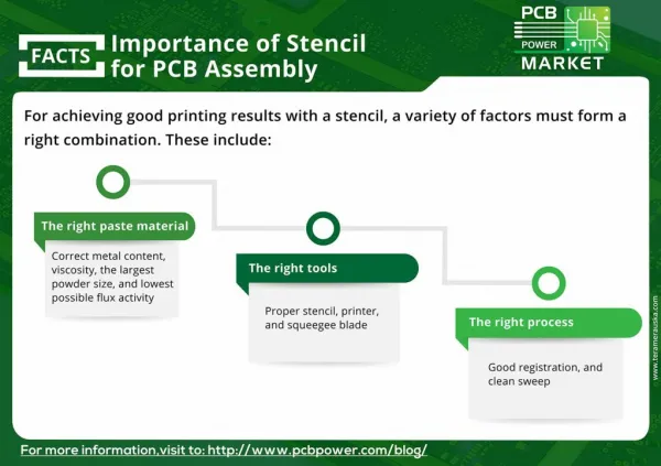
Exemplar Stencils Templates for Computer-Aided Design (CAD) or Gerber-recorded prototypes must conform to the stencil’s unique structure. These can be put to a number of different uses, including manual printing and the modification of various settings to the user’s liking. PCB Stencils With Hybrid Patterns The hybrid PCB stencil is a stencil that is both laser-cut and chemically etched. The utility and durability of the final PCB boards can be compromised, however, if too little solder paste is released throughout the process. Therefore, it combines the best features of both types and could be useful in a variety of settings. How are stencils for PCBs manufactured? In order to place Surface Mount components onto a circuit board, holes or apertures must be cut out of a sheet of hardened steel foil using lasers. Before applying a stencil to a Printed Circuit Board (PCB), a fiducial imprint is used to ensure proper placement. Once the solder paste is in place, it is sliced with a sharp metal tool. Solder paste is spread across a printed circuit board (PCB) and surface-mount components are placed there after being measured and aligned. This indicates that once the PCB stencil has been removed, the components will be able to be positioned on the board in accordance with where they are supposed to go. Important Things to Keep in Mind When Buying PCB Stencil Designs Here are some things to think about when ordering PCB stencils:
Stainless Steel Sheet Depth The stencil’s thickness determines how much solder paste is used, and may be quantified through the opening. Solder paste storage on a board is significantly affected by its thickness and aperture size. Since an excess of solder paste might result in crisscrossing welds, avoiding it is essential. The utility and durability of the final PCB board can be compromised, however, if too little solder paste is released throughout the process. The Depth Of The Doorway By being slightly smaller than the PCB cushion, the aperture of the PCB stencil is made to prevent issues like bridging and the formation of solder beads. When the stencil is released from the board, solder paste may be redistributed across the PCB. It can even be placed upon stencil dividers. Positioning The Stencil To guarantee a precise print of solder paste, “fiducial impressions” or enrollment markings, are added to both the PCB mask and the PCB stencil. These reference points guarantee that the stencil and PCB are aligned properly. Stencil Material The material of the stencil also affects how well solder paste is transferred from the opening or void to the PCB pad. The most common material for PCB stencils is stainless steel. Stencils for PCBs are crucial for maintaining quality control during the assembly of electronic components. They are especially helpful for avoiding malfunctions caused by the accumulation of solder paste or other errors on the PCB board.
Source URL: https://marketguest.com/pcb-rework-stencil-a-comprehensive-guide/


![READ [PDF] Bar Exam Success: A Comprehensive Guide: A Comprehensive Guide (](https://cdn7.slideserve.com/12503608/bar-exam-success-a-comprehensive-guide-dt.jpg)