Download
1 / 30
340 likes | 615 Views
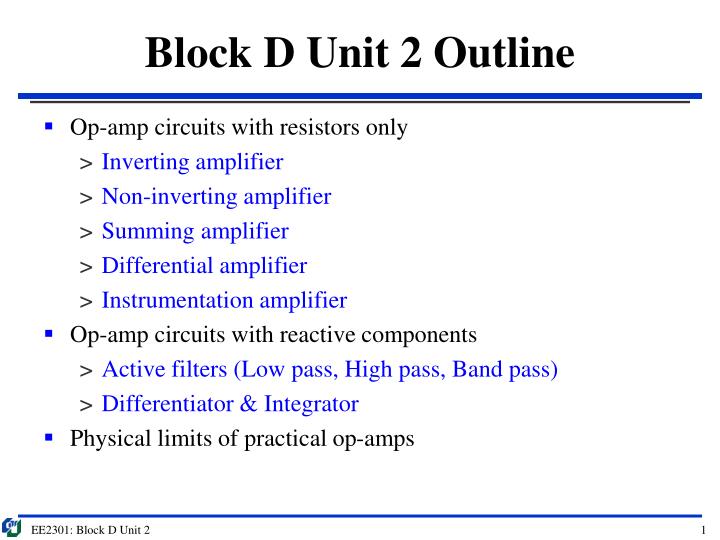
Block D Unit 2 Outline. Op-amp circuits with resistors only Inverting amplifier Non-inverting amplifier Summing amplifier Differential amplifier Instrumentation amplifier Op-amp circuits with reactive components Active filters (Low pass, High pass, Band pass) Differentiator & Integrator

E N D
Block D Unit 2 Outline • Op-amp circuits with resistors only • Inverting amplifier • Non-inverting amplifier • Summing amplifier • Differential amplifier • Instrumentation amplifier • Op-amp circuits with reactive components • Active filters (Low pass, High pass, Band pass) • Differentiator & Integrator • Physical limits of practical op-amps EE2301: Block D Unit 2
Source follower Rs + Vin Vout - RL Find the gain of the above circuit • The key features of the source follower are: • Large input resistance • Small output resistance • Unity gain (i.e. gain of close to one) • It is therefore commonly used as a buffer between a load and source where the impedances are not well matched EE2301: Block D Unit 2
Inverting op amp R2 Note that the inverting input (node X) is at ground R1 and R2 are in series R1 - Vin Applying KCL at X Closed-loop gain Vout + Negative sign indicates a 1800 shift in the phase Gain is set by the resistor values EE2301: Block D Unit 2
R + +_ vin + vout- _ RF RS Non-inverting amplifier iin • Note that since iin = 0: • v+ = vin (no voltage drop across R) • We can apply voltage divider rule to RS & RF iin + vRS- • But we also note that A is infinite, so: • vin = vRS • Hence we then obtain: EE2301: Block D Unit 2
Summing Amplifier RS1 RF Apply NVA at the inverting input terminal: +_ vS1 - RS2 + vout- + +_ vS2 Hence the form of the gain relation can be described by: Vout = -(A1vS1 + A2vS2) A1 and A2 are set by the resistor values chosen. We can extend this result to write a general expression for the gain: EE2301: Block D Unit 2
Differential amplifier R2 One way of analyzing this circuit is to apply superposition (find Vout for V1 or V2 only) R1 V1 - Vout If we short V2 first, we obtain: R1 + V2 R2 R1 V1 - R2 Vout1 + If we short V1 now, we obtain: [R2/(R1+R2)]V2 + Hence, finally: Vout = (R2/R1)(v2 – v1) Output is the difference between the inputs amplified by a factor set by the resistor values. Vout2 - R2 R1 EE2301: Block D Unit 2
Difference amplifier In the case whereby all the resistors are different, as shown in the circuit below, while vout1 remains unchanged, vout2 now becomes: R2 Hence the overall gain expression is given by: R1 V1 - Vout R3 + V2 This is similar to the form of the summing amplifier except that we take the difference between the two inputs: Vout = A2V2 – A1V1 A2 and A1 are set by the resistor values R4 EE2301: Block D Unit 2
Diff Amp: Example 1 Find vout if R2 = 10kΩ and R1 = 250Ω R2 R1 V1 - Vout R1 + V2 R2 EE2301: Block D Unit 2
Diff Amp: Example 2 For the same circuit in the previous example, given v2 = v1: Find vout if v1 and v2 have internal resistances of 500Ω and 250Ω respectively R2 500Ω R1 V1 - Now: R2 = 10kΩ, R1 = 750Ω, R3 = 500Ω, R4 = 10kΩ Vout R1 + V2 250Ω R2 vout = 13.65 v2 – 13.33v1 • We can see that as a result of the source resistances: • Differential gain has changed • vout is not zero for v2 = v1 EE2301: Block D Unit 2
Instrumentation Amplifier + R3 V1 R2 - R1 vo1 + RX Vout - vo2 R1 R2 - V2 + R3 The instrumentation amplifier takes care of this problem by including a non-inverting amplifier (which possesses an infinite input resistance) between the differential amplifier an the inputs. EE2301: Block D Unit 2
Instrumentation Amplifier R3 + Vo1 V1 Vo1 - R1 + RX/2 Vout - Vo2 1st stage comprises a pair of non-inverting amplifiers: Vo1 = (2RX/R1 +1)V1 R3 Closed-loop gain: Vout = (R3/R2)(2RX/R1 + 1)(V2 - V1) 2nd stage is a differential amplifier: Vout = (R3/R2) (Vo2 - Vo1) EE2301: Block D Unit 2
Op amp example 1 Problem 8.5 Find v1 in the following 2 circuits What is the function of the source follower? EE2301: Block D Unit 2
Op amp example 1 solution Fig (a): 6Ω || 3Ω = 2Ω v1 = {2 / (2+6)}*Vg = 0.25Vg Fig (b): Voltage at the non-inverting input = 0.5Vg Voltage at output = Voltage at non-inverting input = 0.5Vg This slide is meant to be blank EE2301: Block D Unit 2
Op amp example 2 Problem 8.7 Find the voltage v0 in the following circuit Transform to Thevenin EE2301: Block D Unit 2
Op amp example 2 solution Thevenin equivalent circuit: Rth = 6 + 2||4 = 22/3 kΩ Vth = {4/(2+4)}*11 = 22/3 V Closed loop gain expression: A = - 12kΩ / Rth (With Vth as input source) Vout = 12/(22/3) * (22/3) = 12V This slide is meant to be blank EE2301: Block D Unit 2
Op amp example 3 R2 Find the closed-loop gain R1 vin - Consider: Current through RB = 0A (Infinite input resistance of op amp) Voltage across RB = 0V Voltage at inverting input = 0V + vout- + RB Same as inverting op amp: A = -R2 / R1 EE2301: Block D Unit 2
Op amp example 4 Find the closed-loop gain R2 Consider: Current through R2 = 0A (Infinite input resistance of op amp) Voltage across R2 = 0V Vout = V- Vout = Vin (Infinite open loop gain of op amp) - + vout- + + vin- EE2301: Block D Unit 2
Common and differential mode A differential amplifier should ideally amplify ONLY DIFFERENCES between the inputs. That is to say identical inputs should give an output of zero. Ideal differential amplifier: Vout = A(V2 – V1) In reality this is not the case as we have seen in a previous example. The output of the amplifier is more accurately described by: Vout = A2V2 + A1V1 A2: Gain when V1 = 0 (V2 is the only input) A1: Gain when V2 = 0 (V1 is the only input) It is then useful to describe the performance of a differential amplifier in terms of the gain when both input are identical (common mode) and when the inputs are equal and out-of-phase (differential) EE2301: Block D Unit 2
Common mode rejection ratio Common mode gain (Acm): Gain when both inputs are exactly the same (V1 = V2 = Vin) Vocm = (A2 + A1)Vin Voltage output for common input Common mode gain (Adm): Gain when both inputs are equal but out-of-phase (V2 = -V1 = Vin) Vodm = (A2 - A1)Vin Voltage output for differential input Divide by 2 since the difference of a pair of differential inputs is twice that of each input The common mode rejection ratio (CMRR) is simply the ratio of the differential mode gain (Adm) over the common mode gain (Acm): CMRR = Adm/Acm A large CMRR is therefore desirable for a differential amplifier EE2301: Block D Unit 2
Active filters Range of applications is greatly expanded if reactive components are used Addition of reactive components allows us to shape the frequency response Active filters: Op-amp provides amplification (gain) in addition to filtering effects Substitute R with Z now for our analysis: ZF and ZS can be arbitrary (i.e. any) complex impedance EE2301: Block D Unit 2
Active low pass filter ZS = RS Amplification Shaping of frequency response EE2301: Block D Unit 2
Active high pass filter ZF = RF Amplification ω→0, Vout/VS → -RF/RS Shaping of frequency response EE2301: Block D Unit 2
Active band pass filter ZS: CS blocks low frequency inputs but lets high frequency inputs through High pass filter ZF: CF shorts RF at high frequency (reducing the gain), but otherwise looks just like a high pass filter at lower frequencies Low pass filter EE2301: Block D Unit 2
Active band pass filter ωHP = 1/(CSRS) – Lower cut-off frequency ωLP = 1/(CFRF) – Upper cut-off frequency For ωHP < ωLP: Frequency response curve is shown below EE2301: Block D Unit 2
Second-order Low Pass Filter R1, R2, C and L are specially chosen so that: ω0 = 1/(CR2) = R1/L. The frequency response function then simplifies to: EE2301: Block D Unit 2
Second-order Low Pass Filter R1, R2, C and L are specially chosen so that: ω0 = 1/(CR2) = R1/L. Above ω0, Hv is reduced by a factor of 100 for a ten fold increase in ω (40dB drop per decade) First-order filter: Hv is reduced by a factor of 10 for a ten fold increase in ω (20dB drop per decade) EE2301: Block D Unit 2
Ideal integrator KCL at inverting input: iS = -iF Virtual ground at inverting input: iS = VS/RS For a capacitor: iF = CF[dVout/dt] Output is the integral of the input EE2301: Block D Unit 2
Ideal differentiator KCL at inverting input: iS = -iF Virtual ground at inverting input: iF = Vout/RF For a capacitor: iS = CS[dVS/dt] Output is the time-differential of the input EE2301: Block D Unit 2
Physical limit: Voltage supply limit The effect of limiting supply voltages is that amplifiers are capable of amplifying signals only within the range of their supply voltages. RS = 1kΩ, RF = 10kΩ, RL = 1kΩ; VS+ = 15V, VS- = -15V; VS(t) = 2sin(1000t) Gain = -RF/RS = -10 Vout(t) = 10*2sin(1000t) = 20sin(1000t) But since the supply is limited to +15V and -15V, the op-amp output voltage will saturate before reaching the theoretical peak of 20V. EE2301: Block D Unit 2
Physical limit: Frequency response limit So far we have assumed in our ideal op-amp model that the open loop gain AV(OL) is infinite or at most a large constant value. In reality, AV(OL) varies with a frequency response like a low pass filter: ω0: frequency when the response starts to drop off The consequence of a finite bandwidth is a fixed gain-bandwidth product If closed loop gain is increased, -3dB bandwidth is reduced Increasing the closed loop gain further results in a bandwidth reduction till the gain-bandwidth produce equals the open-loop gain Gain bandwidth product = A0ω0 EE2301: Block D Unit 2