Download
1 / 9
100 likes | 280 Views
EE314 Microprocessor Systems. Chapter 10. Objectives: The general specification on the 8088 microprocessors The processor’s control signal names and specifications General signal relationship and timings Methods by which the 8088 can interface with external devices

E N D
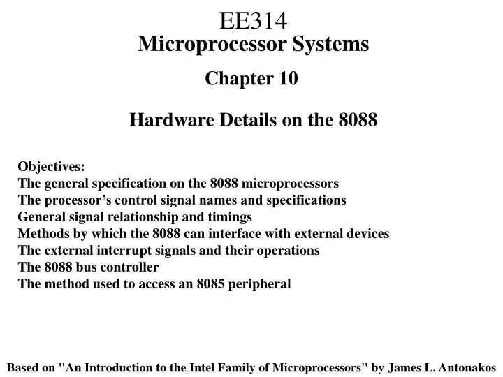
EE314Microprocessor Systems Chapter 10 Objectives: The general specification on the 8088 microprocessors The processor’s control signal names and specifications General signal relationship and timings Methods by which the 8088 can interface with external devices The external interrupt signals and their operations The 8088 bus controller The method used to access an 8085 peripheral Hardware Details on the 8088 Based on "An Introduction to the Intel Family of Microprocessors" by James L. Antonakos
10.3 CPU pin descriptions Minmode operation signals (MN/MX=1) Time-multiplexed Address Bus /Status signals (outputs) 0V=“0”, reference for all voltages GND A14 A13 A12 A11 A10 A9 A8 AD7 AD6 AD5 AD4 AD3 AD2 AD1 AD0 NMI INTR CLK GND 1 40 8088 20 21 Vcc A15 A16/S3 A17/S4 A18/S5 A19/S6 ___ SS0 (HIGH) ___ MN/MX ___ RD ___ ____ HOLD (RQ/GT0) ___ ____ HLDA (RQ/GT1) ___ ______ WR(LOCK) __ __ IO/M(S2) __ __ DT/R(S1) ____ __ DEN(S0) ALE (QS0) _____ INTA (QS1) _____ TEST READY RESET 5V±10% Maxmode operation signals (MN/MX=0) Address Bus (outputs) Control Bus (in,out) Operation Mode, (input): 1 = minmode (8088 generates all the needed control signals for a small system), 0 = maxmode (8288 Bus Controller expands the status signals to generate more control signals) Time-multiplexed Address (outputs)/Data Bus (bidirectional) Status signals (outputs) Hardware interrupt requests (inputs) 2...5MHz, 1/3 duty cycle (input) Interrupt acknowledge (output)
10.3 CPU pin descriptions MEMRD RD MEMWR WR IORD Decoding 8088 memory and I/O read/write signals IOWR IO/M 8088 Status Signals 8088 Signal Summary Comparison of NMI and INTR
10.4 The 8284 Clock Generator 5V READY1 CLK 8088 READY RESET RDY1 RDY2 EFI CLK F/C CSYNC AEN1 AEN2 8284 ASYNC X1READY X2RESRESET READY2 0 = crystal oscillator 1 = TTL clock on EFI, synchronized on CSYNC 4K7 qualifiers for READY1,-2 5V 2X510 1 = one WAIT state forced by READY CLK 10MHz 100K 0 = forces the P to froze the current bus cycle inserting WAIT STATES (all signals keep their values), allowing slower devices time to properly answer. 10F 5V 1N4148 1/3 fosc 1/3 duty cycle RES [V] t X1,2 [V] RESET 1L 0L t t
10.5 The 8288 Bus Controller 74LS244 G1 G2 CPU Address Bus (A16-A19, if needed, should be latched the same way like AD0-AD7) Identify the Memory Byte (one of 220 (216 in example)) OR the I/O port (one of 216) to be read OR write in the current bus cycle A8-A15 AD0-AD7 8088 S0 S1 S2 8282 STB OE D Q LE Advanced Write Commands, providing additional access time for the selected circuit Data to be transferred in the current bus cycle 8286 OE T Max one active at a time, identifying Memory vs. I/O and Read vs. Write CPU Data Bus Data Transmit/Receive DENDT/RMRDC ALEMWTC S0IORC S1 8288 IOWC S2INTA AMWC AIOWC IOB AEN CEN Address Latch Enable Status Signals (codify the bus cycle type) 5V Command Enable Control Bus Address Enable I/O Bus only CLK Data Enable Memory ReaD Command Memory WriTe Command Input/Output Read Command Input/Output Write Command INTerrupt Acknowledge Advanced Memory Write Command Advanced Input/Output Write Command
10.6 System Time Diagrams - CPU Bus Cycle T1 T2 T3 TW T4 CLK ALE Address latches store the actual values Memory Cycle (I/O cycle is similar but IO/M = 1) IO/M A16- A19 A16-A19 S3- S6 A8- A15 A8- A15 READY the P samples READY (if 0 a WAIT state follows) The slow device drives READY= 0 Read Cycle (instruction fetch and memory operand read) RD P reads Data Bus AD0- AD7 A0- A7 D0- D7 (Data in) Tri-state DT/R Direction “READ” for the Data Buffer DEN Enables Data Buffer Memory reads Data Bus WR Write Cycle (memory operand write) AD0- AD7 A0- A7 D0- D7 (Data out) DT/R Direction “READ” for the Data Buffer DEN Enables Data Buffer
Maxmode Interrupt acknowledge timing T1 T2 T3 T4 T1 T2 T3 T4 CLK LOCK Prevents P to enter a HOLD state INTA AD0- AD7 INT type Tri-state Second INTA cycle First INTA cycle two INTA cycles in maxmode, the device requesting INT has to drive the “INT type” on the Data Bus, during the second cycle. Minmode Interrupt acknowledge timing T1 T2 T3 T4 CLK a single INTA cycle in minmode. INTA HOLD/HLDA Timing AD0- AD7 INT type Tri-state T4 T1 CLK only after ending the current bus cycle HOLD HOLD state: the P releases the Address, Data, Control and Status buses (these pins are tri-sated (high impedance) HLDA 10.6 System Time Diagrams - INT and HOLD
10.7 Personal Computer Bus Standards I/O Bus PCI (Mezzanine) Bus Medium Complexity PC Architecture CPU P Bus Simple P System Architecture Cash Memory Memory Controller Main Memory Memory Bus CPU P Bus I/O Bus Controller Plug-in I/O Boards Memory I/O - ISA = Industry Standard Architecture (8 data bits = PC-XT bus, or 16 data bits = PC-AT bus) - EISA = Extended ISA - MCA = Micro Channel Architecture (only IBM) Motherboard I/O Circuits PCI (Peripheral Component Interconnect bus) based Architecture CPU P Bus Cash Memory Memory Controller Main Memory Memory Bus Motherboard- and Fast Plug-in I/O Circuits Bridge Controller I/O Bus Controller Slow Plug-in I/O Boards I/O Bus
GND RESETDRV +5V IRQ2(9) -5V DRQ2 -12V 0WS +12V GND -SMEMW -SMEMR -IOW -IOR -DACK3 DRQ3 -DACK1 DRQ1 -REFRESH SYSCLK IRQ7 IRQ6 IRQ5 IRQ4 IRQ3 -DACK2 TC BALE +5V OSC GND B1 A1 B5 A5 B10 A10 B15 A15 B20 A20 B25 A25 B30 A30 B31 A31 I/O CH CK SD7 SD6 SD5 SD4 SD3 SD2 SD1 SD0 I/O CH RDY AEN SA19 SA18 SA17 SA16 SA15 SA14 SA13 SA12 SA11 SA10 SA9 SA8 SA7 SA6 SA5 SA4 SA3 SA2 SA1 SA0 -MEMCS16 -IOCS16 IRQ10 IRQ11 IRQ12 IRQ15 IRQ14 -DACK0 DRQ0 -DACK5 DRQ5 -DACK6 DRQ6 -DACK7 DRQ7 +5V -MASTER GND D1 C1 D5 C5 D10 C10 D15 C15 D18 C18 SBHE LA23 LA22 LA21 LA20 LA19 LA18 LA17 -MEMR -MEMW SD8 SD9 SD10 SD11 SD12 SD13 SD14 SD15 Back side of PC B31 B1 A31 A1 10.7 Personal Computer Bus Standards - ISA Bus D18 D1 C18 C1