Download
1 / 7
70 likes | 75 Views
Embedded software development services are advancing quickly now. Being essential for independent frameworks prior, presently it stretches out to web, cloud, and portable. These advancements change the manner in which clients cooperate with the item. The CAD drafting services help to integrate complex designs with various techniques and accelerate the drafting process. Thus, these services improve the efficiency of the process, presentation styles, CAD standards, and many more.<br><br>Visit: https://www.sunstreamglobal.com/services/embedded-development/

E N D
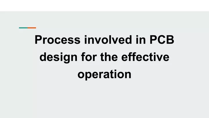
Process involved in PCB design for the effective operation
The modern lights have pushed down the old incandescent light by this PCB board. The PCB design companies manufacturers use metal such as aluminum boards for a circuit to give less heat and efficient thermal transfer. Hence, PCB is the main brain behind every electronic device. The well-designed and manufactured board will effectively reduce the possibility of errors and prevent the device from getting short-circuited.
Creating a schematic design of the project is drawing the blueprint of the device like designing components, their connection, and many more. The user can get the illustration by using CAD drafting services for more accuracy.
Create a PCB layout: Developing the PCB layout is much easier than creating a schematic representation of the PCB board. A good PCB designer will work on different platforms like Altium, Allegro, and many more to show how the illustration will work effectively according to the layout.
Create a PCB layout Developing layout is much easier than creating schematic representation PCB board. the PCB a of the
They need not use all the components designed in the PCB board and can select the elements according to the rules that need to be manufactured. Steel detailing company make sure that their products have the PCB stack up according to the guidelines for a better understanding of the materials