Download
1 / 19
190 likes | 298 Views
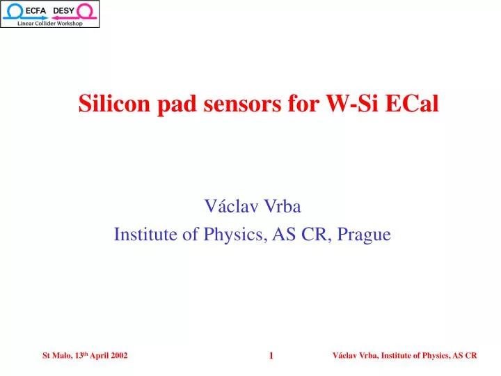
Silicon pad sensors for W-Si ECal. Václav Vrba Institute of Physics , AS CR, Prague. Outline. Sensor tile outer dimensions Pad array design consideration Time schedule - towards the first prototype Tests outlines. Sensor tile outer dimensions. Outcome from the meeting at EP:

E N D
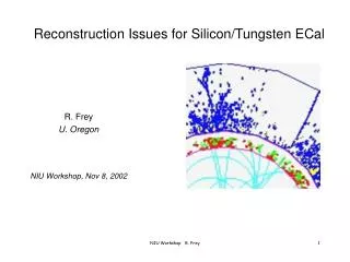
Silicon pad sensors for W-Si ECal Václav Vrba Institute of Physics, AS CR, Prague Václav Vrba, Institute of Physics, AS CR
Outline • Sensor tile outer dimensions • Pad array design consideration • Time schedule - towards the first prototype • Tests outlines Václav Vrba, Institute of Physics, AS CR
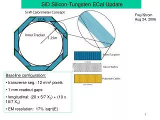
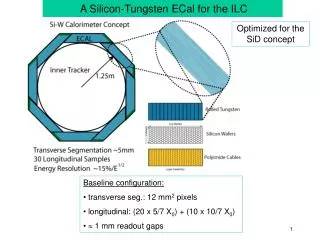
Sensor tile outer dimensions • Outcome from the meeting • at EP: • 4” high resistivity wafers • tile side: 62.0+0.0 • -0.1 mm • scribe line: 100 m • scribe safety zone: 200 m • guard ring width: cca 750 m (cca 1.5 * wafer thickness) • The dead zone width is about 1 mm 1.0 mm Wafer book keeping information Václav Vrba, Institute of Physics, AS CR
Pad array design consideration Along with the diodes, the technique used for fabrication of bias resistors and coupling capacitors represents an important issue: a) polysilicon resistors – production of the tile needs about 7-8 masks; can be the source of additional yield reduction. b) punch through resistors – production of the tile needs about 5 masks; easy to produce – needs to check whether required parameters can be achieved. c) deposited resistors (amorphous silicon) – achievement of EP; - needs about 4-5 masks for production of the diodes array; on top of that additional fabrication of resistor and capacitors. d) ion implantation resistors – not considered here. Václav Vrba, Institute of Physics, AS CR
Design consideration: Polysilicon resistors Bias lines Top view Direct contact on diode – e.g. for testing Bias resistor Coupling capacitor Vertical cross section Václav Vrba, Institute of Physics, AS CR
Design consideration: Polysilicon resistors Václav Vrba, Institute of Physics, AS CR
Design consideration: Punch through resistors Bias lines Top view Direct contact on diode – e.g. for testing Bias resistor Coupling capacitor Vertical cross section Václav Vrba, Institute of Physics, AS CR
Deposited resistors – before deposition Václav Vrba, Institute of Physics, AS CR
Deposited resistors – after deposition Bias lines e.g.Wire bonding, Flex cable gluing, etc. Václav Vrba, Institute of Physics, AS CR
Design consideration: a partial summary a) polysilicon resistors: • should not be a problem to have resistors 10 M; • capacitors 1-10 nF. b) punch through resistors: • resistors to be tested; if acceptable then it is a simple solution; • capacitors as a). c) deposited resistors: • will be considered in the first prototype submission to test the deposition technology of capacitors and resistors Compatibility of process for variants a), b) and c) on one wafer? To try all variants separately could be quite costly! Option c) as a baseline for main sensor tile? Václav Vrba, Institute of Physics, AS CR
Design consideration: a partial summary Václav Vrba, Institute of Physics, AS CR
Time schedule now in process By end of April 2002 By end of June 2002 • Pre-prototyping • using existing masks to evaluate some effects of: • high resistive Silicon; • guard rings, scribe lines, etc. • #wafers thickness [m] • 4 SSP Wacker 500 • 3 DSP Topsil 500 • 4 DSP Topsil 300 • Mask design preparation GDS file • First 10-16 wafers ready for testing Václav Vrba, Institute of Physics, AS CR
Pre-prototyping Active area cca 0.3 cm2 Active area cca 10 cm2 Wafer diameter: 100 mm Wafer backside all Al metallized Václav Vrba, Institute of Physics, AS CR
Tests outlines A) Diode tests a) C-V curves: • determination of Vfull-depletion; Vop = Vfull-depletion + 50 V. b) I-V curves: • Vbreak-down Vop • Ileak @ Vop < cca 30 nA/cm2 c) Long term stability tests: • Ileak @ Vop . Tile should be rejected if: • Vbreak-down< Vop • Ileak > I crit (to be defined). Václav Vrba, Institute of Physics, AS CR
Electric characterization Václav Vrba, Institute of Physics, AS CR
Long term current stability on Tile Measured @ 150V x 10s time Václav Vrba, Institute of Physics, AS CR
Tests outlines B) Bias resistors a) shorts b) breaks c) outside specifications C) Capacitance couplings a) shorts b) breaks c) outside specifications Václav Vrba, Institute of Physics, AS CR
Manual Probestation Václav Vrba, Institute of Physics, AS CR
Manual Probestation Václav Vrba, Institute of Physics, AS CR