Download
1 / 96
960 likes | 975 Views
Chapter 11 - DAC Testing. Basics of Converter Testing Intrinsic Parameters Versus Transmission Parameters

E N D
Basics of Converter Testing • Intrinsic Parameters Versus Transmission Parameters • Chapter 8, “Analog Channel Testing” and Chapter 9, “Sampled Channel Testing”, discussed common channel parameters such as gain, gain tracking, signal to noise ratio (SNR), and signal to distortion ratio (S/D). • These parameters are called transmission parameters, or performance parameters, since they describe the effect of the analog or sampled channel on the quality of transmitted signals such as voice or modulated data. • In both analog and sampled channels, transmission parameters are determined by the quality of all the channel’s subcircuits
Basics of Converter Testing • Intrinsic Parameters Versus Transmission Parameters • In this chapter, we will focus on the so called intrinsic parameters of DACs • such as absolute error • integral non-linearity (INL) and differential non-linearity (DNL). • Intrinsic parameters are those parameters that are intrinsic to the circuit itself. They are not dependent on the nature of the test stimulus.
Basics of Converter Testing • Intrinsic Parameters Versus Transmission Parameters • When testing a DAC or ADC it is common to measure both intrinsic parameters and transmission parameters for full characterization. • It is often unnecessary to perform both transmission tests and intrinsic tests in production. • Production testing strategy is often determined by the end use of the DAC or ADC • Unlike digital circuits which can be tested based on what they are (NAND gate, flip-flop, counter, etc.), mixed-signal circuits are often tested based on what they do in the system-level application (precision voltage reference, audio signal reconstructor, video signal generator, etc.).
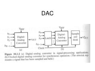
Basics of Converter Testing • Comparison of DACs and ADCs • Although this chapter is devoted to DAC testing, many DAC concepts are closely tied to ADC testing. • For instance, the code-to-voltage transfer characteristics for DACs are similar to the voltage-to-code characteristics of ADCs. • It is very important to note that a DAC represents a one-to-one mapping function whereas an ADC represents a many-to-one mapping. • For each digital code, a DAC produces only one output voltage. An ADC, by contrast, produces the same output code for a range of input voltages.
Basics of Converter Testing • Comparison of DACs and ADCs • The difference between DAC and ADC transfer characteristics prevents us from using complementary testing techniques on DACs and ADCs • We will concentrate mostly on voltage output DACs. Current output DACs are tested using the same techniques, using either a current mode DC voltmeter or a calibrated voltage-to-current translation circuit located on the device interface board (DIB).
Basics of Converter Testing • DAC Failure Mechanisms • There are many different types of DACs • binary weighted architectures • resistive divider architectures • pulse width modulated (PWM) architectures • pulse density modulated (PDM) architectures (commonly known as Sigma Delta DACs). • hybrids of these architectures such as the multi-bit Sigma Delta DAC and segmented resistive divider DACs. • Each of these DAC architectures has a unique set of strengths and weaknesses. • Each architecture’s weaknesses determine its likely failure mechanisms, and test methodology
Basic DC Tests • Code Specific Parameters • DAC specifications sometimes require specific voltage levels correspond to specific digital codes • Common code-specific parameters include the maximum full scale (+FS) voltage, minimum full scale (-FS) voltage, and midscale (MS) voltage. • The midscale voltage typically corresponds to 0V in bipolar DACs or a center voltage such as Vdd/2 in unipolar (single power supply) DACs. • It is important to note that although the minimum full scale voltage is often designated with the –FS notation, it is not necessarily a negative voltage.
Basic DC Tests • Full Scale Range • Full scale range (FSR) is defined as the voltage difference between the maximum voltage and minimum voltage that can be produced by a DAC. • Typically measured by simply measuring the DAC’s +FS voltage, then measuring the DAC’s –FS voltage and subtracting using the equation: • FSR = +FS Voltage - -FS Voltage
Basic DC Tests • DC Gain, Gain Error, Offset, and Offset Error • It is tempting to say that the DAC’s offset is equal to the measured midscale voltage. • It is also tempting to define the gain of a DAC as the full scale range divided by the number of spaces, or steps, between codes. • These definitions of offset and gain are approximately correct. In fact, they are sometimes defined in spec sheets exactly this way. • These definitions would be quite valid in a perfectly linear DAC. However, in an imperfect DAC they are inferior because they are very sensitive to variations in the –FS, MS, and +FS voltage outputs.
Basic DC Tests • DC Gain, Gain Error, Offset, and Offset Error • 0 code does not produce 0 V as it should - the overall curve has an offset near 0V. • Notice that the gain, if defined as the full scale range divided by the number of spaces between codes doesn’t match the general slope of the curve.
Basic DC Tests • DC Gain, Gain Error, Offset, and Offset Error • A less ambiguous definition of gain and offset can be found by computing the best-fit line for these points and then computing the gain and offset of this line. • The best-fit line approach is independent of DAC resolution, so it is the preferred technique. • A best-fit line is commonly defined as the line having the minimum squared errors between its evenly spaced samples and the actual DAC output samples
Basic DC Tests • DC Gain, Gain Error, Offset, and Offset Error • Best Fit Linei = Slope * i + Offset Unlike the gain calculated from the full scale range divided by the number of code transitions, the slope of the best-fit line represents the true gain of the DAC. It is based on all samples in the DAC transfer curve and therefore is not terribly sensitive to any one code’s location
Basic DC Tests • DC Gain, Gain Error, Offset, and Offset Error • Gain error, expressed as a percent, is defined using the following formula: • Gain Error (percent) = 100* ( (Actual Gain / Ideal Gain) – 1) • The best-fit line’s calculated offset is not dependent on a single code as it is in the midscale code method. Instead, the best-fit line offset represents the offset of the total sample set. • The DAC’s offset is defined as the voltage at which the best-fit line crosses the y-axis. The DAC’s offset error is equal to its offset minus the ideal voltage at this point in the DAC transfer curve
Basic DC Tests • LSB Step Size • The least significant bit (LSB) step size is defined as the average step size of the DAC transfer curve. • It is equal to the gain of the DAC, in volts per bit. • It is possible to measure the approximate LSB size by simply dividing the full scale range by the number of code transitions • It is more accurate to measure the gain of the best-fit line to calculate the average LSB size
Basic DC Tests • DC PSS • DAC DC power supply sensitivity (PSS) is easily measured by applying a fixed code to the DAC’s input and measuring the DC gain from one of its power supply pins to its output. • PSS for a DAC is therefore identical to the measurement of PSS in any other circuit, as described in Chapter 3. • The only difference is that a DAC may have different PSS performance depending on the applied digital code. • Usually, a DAC will have the worst PSS performance at its full scale and/or minus full scale settings, because these settings tie the DAC output directly to a voltage derived from the power supply. • Worst-case conditions should be used once they have been determined through characterization of the DAC.
Transfer Curve Tests • Absolute Error • The ideal DAC transfer curve is one in which the step size between each output voltage and the next is exactly equal to the desired LSB step size. • Of course, physical DACs don’t behave in an ideal manner, so we have to define figures of merit for their actual transfer curves. • One of the simplest figures of merit is the DAC’s maximum and minimum absolute error. • An absolute error curve is calculated by subtracting the ideal DAC output curve from the actual measured DAC curve. The values in the absolute error curve can be converted to LSBs by dividing each voltage by the ideal LSB size. The conversion from volts to LSBs is a process called normalization.
Transfer Curve Tests • Monotonicity • A monotonic DAC is one in which each voltage in the transfer curve is larger than the previous voltage, assuming a rising voltage ramp for increasing codes. • If the voltage ramp decreases with increasing code values, we simply have to make sure that each voltage is less than the previous one. • Monotonicity testing requires that we take the discrete first derivative of the transfer curve and make sure that each value is positive (for rising ramps) or negative (for falling ramps). • The discrete derivative is calculated by simply subtracting each value Si from the next value Si+1.
Transfer Curve Tests • Differential Non-Linearity • In a perfect DAC, each step would be exactly the ideal LSB step size. Differential non-linearity (DNL) is a figure of merit that describes the uniformity of the LSB step sizes between DAC codes. • DNL is also known as differential linearity error (DLE). • The DNL curve represents the error in each step size, expressed in fractions of an LSB. • DNL is calculated by computing the discrete first derivative of the DACs transfer curve, then normalizing the derivative curve to one LSB, and finally subtracting one LSB from the normalized derivative curve
Transfer Curve Tests • Differential Non-Linearity • Three basic types of DNL calculations: best-fit, endpoint, and absolute, depending on the method of defining LSB. • Best-fit DNL uses the best-fit line’s slope to calculate the average LSB size. • Uses gain errors in the DAC without relying on the values of a few individual voltages (best method). • Endpoint DNL is calculated by dividing the full scale range by the number of transitions. • Depends on the value of the maximum full scale and minimum full scale DAC output levels. • highly sensitive to errors in these two values, and is less ideal than the best-fit technique. • Finally, the absolute DNL technique uses the ideal LSB size. This technique is not commonly used, since it assumes the DAC’s gain is close to ideal.
Transfer Curve Tests • Integral Non-Linearity • The integral non-linearity (INL) curve is a comparison between the actual DAC curve and one of three lines: the best-fit line, the endpoint line, or the ideal DAC line. • The INL curve, like the DNL curve, is normalized to the LSB step size. • As in the DNL case, the best-fit line is the preferred reference line, since it eliminates sensitivity to individual DAC values.
Transfer Curve Tests • Integral Non-Linearity • The INL curve can be calculated by subtracting the best-fit (or endpoint or ideal) DAC line from the actual DAC curve, dividing the results by the average LSB step size. • Note that using the ideal DAC line is equivalent to calculating the absolute error curve. • As in DNL testing, we are interested in the maximum and minimum value in the INL curve, which we compare against a limit such as +/- ½ LSB.
Transfer Curve Tests • Integral Non-Linearity • The INL curve can also be calculated by integrating the DNL curve, thus the term “integral non-linearity”. DNL is a measurement of how consistent the step sizes are from one code to the next. • INL is therefore a measure of accumulated errors in the step sizes. Thus, if the DNL values are consistently larger than zero for many codes in a row (step sizes are larger than 1 LSB), the INL curve will exhibit an upward trend. Likewise, if the DNL is less than zero for many codes in a row, the INL curve will exhibit a downward trend. Ideally, the positive error in one code’s DNL will be balanced by negative errors in surrounding codes and vice versa. If this is true, then the INL curve will tend to remain near zero. If not, the INL curve may exhibit large upward or downward bends, causing INL failures.
Transfer Curve Tests • Integral Non-Linearity • The INL integration is implemented using a running sum of the elements of the DNL. The ith element of the INL curve is equal to the sum of the first i-1 elements of the DNL curve plus a constant of integration. • When using the best-fit method, the constant of integration is equal to the difference between the first DAC output voltage and the corresponding point on the best-fit curve. • When using the endpoint method, the constant of integration is equal to zero. • When using the absolute method, the constant is set to the difference between the first and ideal DAC outputs. • In any running sum calculation it is important to use high precision mathematical operations to avoid accumulated error in the running sum.
Transfer Curve Tests • Integral Non-Linearity • Conversely, DNL can be calculated by taking the first derivative of the INL curve. • This is usually the easiest way to calculate DNL when testing DACs, but we will see in the next chapter that the DNL curve for an ADC is easier to capture than the INL curve. • In ADC testing it is more common to calculate the DNL curve first, and then integrate it to derive the INL curve.
Problem: • A 4-bit two’s complement DAC produces the following set of voltage levels, starting from code –8 and progressing through code +7: • -780 mV, -705 mV, -530 mV, -455 mV, -400 mV, -325 mV, -150 mV, -75 mV, 120 mV, 195 mV, 370 mV, 445 mV, 500 mV, 575 mV, 750 mV, 825 mV. • These code levels are shown in . Calculate the best-fit line’s gain and offset. The ideal DAC output at code 0 is 0 V. The ideal gain is equal to 100 mV / bit. Calculate the DAC’s gain (volts per bit), gain error, offset, and offset error.
Solution: • We calculate gain and offset resulting in a gain value of 109.35 mV / bit and an offset value of –797.64 mV. The gain is equal to 109.35 mV and the gain error is given by the equation: Gain Error (%) = 100 * ((109.35 mV / 100 mV) –1 ) = 9.35% • Because this DAC uses a two’s complement encoding scheme, the offset value is the offset of the best-fit line, not the offset of the DAC. The DAC’s offset is found by calculating the best-fit line’s value at DAC code 0, which corresponds to data point = 8. • DAC Offset = 8 * Gain + Offset = 8 * 109.35 mV – 797.64 mV= 77.16 mV • DAC Offset Error = DAC Offset – Ideal Offset • =77.16 mV – 0 V = 77.16 mV
Problem: • Assuming an ideal gain of 100 mV per LSB and an ideal offset of 0 V at code 0, calculate the absolute error curve for the 4-bit DAC of the previous example. Normalize these error values to convert the error curve to LSBs
Solution: • The ideal DAC levels are –800 mV, -700 mV, ...+700 mV. Subtracting these ideal values from the actual values, we can calculate the absolute voltage errors: • +20 mV, -5 mV, +70 mV, +45 mV, 0 mV, -25 mV, +50 mV, +25 mV, +120 mV, +95 mV, +170 mV, +145 mV, +100 mV, +75 mV, +150 mV, +125 mV. • The maximum absolute error is +170 mV and the minimum absolute error is –25 mV. Dividing each value by the ideal LSB size (100 mV), we get the normalized error curve shown on the next slide.
This curve shows that this DAC’s maximum and minimum absolute errors are +1.7 LSBs and –0.25 LSBs
Problem: • Verify monotonicity in the previous DAC example. • Solution: • The first derivative of the DAC transfer curve is calculated, yielding the following values: • 75 mV, 175 mV, 75 mV, 55 mV, 75 mV, 175 mV, 75 mV, 195 mV, 75 mV, 175 mV, 75 mV, 55 mV, 75 mV, 175 mV, 75 mV • Since each value has the same sign (positive), the DAC is monotonic. • Notice that there are only 15 first derivative values, even though there are 16 codes in a 4-bit DAC. This is the nature of the discrete derivative, since there one fewer changes in voltage than there are voltages.
Problem: • Calculate the DNL curve for the 4-bit DAC of the previous examples. Use the best-fit line to define the average LSB size. Does this DAC pass a +/- ½ LSB specification for DNL?
Solution: • The first derivative of the transfer curve was calculated in the previous monotonicity example. The first derivative values are: 75 mV, 175 mV, 75 mV, 55 mV, 75 mV, 175 mV, 75 mV, 195 mV, 75 mV, 175 mV, 75 mV, 55 mV, 75 mV, 175 mV, 75 mV. • The average LSB size, using the best-fit line calculation was 109.35 mV. Dividing each step size by the average LSB size yields the normalized derivative curve (in LSBs): 0.686, 1.6, 0.686, 0.503, 0.686, 1.6, 0.686, 1.783, 0.686, 1.6, 0.686, 0.503, 0.686, 1.6, 0.686. • Subtracting one LSB from each of these values gives us the DNL curve for this DAC: -0.314, 0.6, -0.314, -0.497, -0.314, 0.6, -0.314, 0.783, -0.314, 0.6, -0.314, -0.497, -0.314, 0.6, -0.314.
shows the DNL curve for this DAC. The maximum DNL value is +0.783 LSB, while the minimum DNL value is –0.314. The minimum value is greater than –½ LSB, but the maximum DNL value is greater than ½ LSB. Therefore, this DAC fails the DNL specification of +/- ½ LSB.
Problem • Calculate the INL curve for the 4-Bit DAC in the previous examples. First use an endpoint calculation, then use a best-fit calculation. Does either result pass a specification of +/- ½ LSB? Do the two methods produce a significant difference in results?
Solution: • Using an endpoint calculation method, the INL curve for the 4-bit DAC of the previous examples is calculated by subtracting a straight line between the –FS voltage and the +FS voltage from the DAC output curve. The difference at each point in the DAC curve is divided by the average LSB size, which in this case is calculated using an endpoint method. As in the endpoint DNL example, the average LSB size is equal to 107 mV. • The results of the INL calculations are listed below. Again, these values are expressed in LSBs. • 0, -0.299, 0.336, 0.037, -0.449, -0.748, -0.112, -0.411, 0.411, 0.112, 0.748, 0.449, -0.37, -0.336, 0.299, 0
The figure shows the endpoint INL curve. The maximum INL value is +0.748 LSB, and the minimum INL value is –0.748. This DAC does not pass an INL specification of +/- ½ LSB
Best Fit Solution • Using a best-fit calculation method, the INL curve for the 4-bit DAC of the previous examples is calculated by subtracting the best-fit line from the DAC output curve. • Each point in the difference curve is divided by the average LSB size, which in this case is calculated using the best-fit line method. As in the best-fit DNL example, the average LSB size is equal to 109.35 mV. The results of the INL calculations are listed below, expressed in LSBs. • 0.161, -0.153, 0.448, 0.133, -0.364, -0.678, -0.077, -0.392, 0.392, 0.077, 0.678, 0.364, -0.133, -0.448, 0.153, -0.161 • The best-fit INL curve is shown for comparison with the endpoint INL curve. The maximum value is +0.678 and the minimum value is –0.678.
The best-fit INL results are better than the endpoint INL values, but still do not pass a +/- ½ LSB test limit. The two INL curves are somewhat similar in shape, but the individual INL values are quite different. • The choice of calculation technique is much more important for INL curves than for DNL curves. • A best-fit curve will usually give better INL results than an endpoint INL calculation
Transfer Curve Tests • Partial Transfer Curves • Nothing prevents a customer or systems engineer from requesting that only a portion of a DAC or ADC transfer curve meet certain specifications. For example, a DAC may be designed so that its –FS code corresponds to 0 V. However, due to analog circuit clipping as the DAC output signal approaches ground, the DAC may clip to a voltage of 100 mV. If the DAC is designed to perform a specific function that never requires voltages below 100 mV, then the customer may not care about this clipping. In such a case, the DAC codes below 100 mV are excluded from the offset, gain, INL, DNL, etc. specifications.
Transfer Curve Tests • Major Carrier Testing • The techniques discussed thus far for measuring INL and DNL are based on a testing approach called all-codes testing. In all-codes testing, all valid codes in the transfer curve are measured to determine the INL and DNL values. Unfortunately, all-codes testing can be a very time consuming process. Depending on the architecture of the DAC, it may be possible to determine the location of each voltage in the transfer curve without measuring each one explicitly. We will refer to this as selected-code testing. Selected-code testing can result in significant test time savings, which of course represents a substantial savings in test cost. There are several selected-code testing techniques, the simplest of which is called the major carrier method.
Transfer Curve Tests • Major Carrier Testing • Many DACs are designed using an architecture in which a series of binary weighted resistors or capacitors are used to convert the individual bits of the converter code into binary weighted currents or voltages. These currents or voltages are summed together to produce the DAC output. • For instance, a binary weighted unsigned binary DAC’s output can be described as a sum of binary weighted voltage or current values, W0, W1, ... Wn, multiplied by the individual bits of the DAC’s input code, D0, D1, ... Dn. The DAC’s output value is output = D0*W0+D1*W1+...+Dn*Wn + DC Base • where: DAC code bits D0-Dn take on the value of 1 or 0; W1 = 2*W0; W2 = 2*W1 … Wn = 2*Wn-1 • DC Base is the DAC output value with a -FS input code
Transfer Curve Tests • Major Carrier Testing • If this idealized model of the DAC is sufficiently accurate, then we only need to measure the values of W0, W1, ... Wn to predict every voltage in the DACs transfer curve. • This DAC testing method is called the major carrier technique. • The major carrier approach can be used for ADCs as well as DACs. • The assumption of sufficient DAC or ADC model accuracy is only valid if the actual superposition errors of the DAC or ADC are low. • The superposition assumption can only be determined through characterization, comparing the all-codes DAC output levels with the ones generated by the major carrier method.
Transfer Curve Tests • Major Carrier Testing • The most straightforward way to measure the value W0 is to set DAC code bit D0 to one and all other bits to zero. Likewise, the other major carrier values Wn can be measured by setting Dn to one and all other bits to zero. • However, the resulting output levels are widely different in magnitude. This makes them difficult to measure accurately with a voltmeter, since the voltmeter’s range must be adjusted for each measurement.
Transfer Curve Tests • Major Carrier Testing • A better approach that alleviates the accuracy problem is to measure the step size of the major carrier transitions in the DAC curve, which are all approximately 1 LSB in magnitude. A major carrier transition is the voltage (or current) transition between the DAC codes 2n-1 and 2n. For example, the transition between binary 00111111 and 01000000 is a major carrier transition. Major carrier transitions can be measured using a voltmeter’s sample-and-difference mode, giving highly accurate measurements of the major carrier transition step sizes.
Transfer Curve Tests • Major Carrier Testing • Once the step sizes are known, we can use a series of inductive calculations to find the values of W0, W1, ... Wn. We start by realizing that we have actually measured the following values: • DC Base = Measured DAC output with minus full scale code • V0 = W0 • V1 = W1 – W0 • V2 = W2 – (W1+W0) • V3 = W3 – (W2+W1+W0) • ... • Vn = Wn – (Wn-1+Wn-2+Wn-3...W0)
Transfer Curve Tests • Major Carrier Testing • The value of the first major transition, V0, is a direct measurement of the value of W0 (the step size of the least significant bit). The value of W1 can be calculated by rearranging the second equation: W1 = V1 + W0. Once the values of W0 and W1 are known, the value of W2 is calculated by rearranging the third equation: W2 = V2 + W1 + W0, and so forth. Once the values of W0-Wn are known, the complete DAC curve can be reconstructed using the original model of the DAC. The DAC model’s output is calculated for each possible combination of input bits D0-Dn • DAC Output = D0*W0+D1*W1+...+Dn*Wn + DC Base
Transfer Curve Tests • Major Carrier Testing • The major carrier technique can also be used on signed binary and two’s complement converters, although the codes corresponding to the major carrier transitions must be chosen to match the converter encoding scheme. Aside from minor modifications in code selection, the major carrier technique is the same as the simple unsigned binary approach