Download
1 / 30
700 likes | 1.67k Views
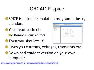
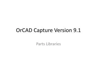
Orcad 9.2. Embedded System Project. Orcad Capture. Capture is an electronic design environment Capture is used to draw a schematic design of your electronic device Logical connections Part symbols Starting Orcad Capture (in Windows) Start – Programs – Cadence PSD – Capture. Orcad Layout.

E N D
Orcad 9.2 Embedded System Project
Orcad Capture • Capture is an electronic design environment • Capture is used to draw a schematic design of your electronic device • Logical connections • Part symbols • Starting Orcad Capture (in Windows) • Start – Programs – Cadence PSD – Capture
Orcad Layout • Layout is a circuit board layout tool • Layout is used to design the physical printed circuit board (PCB) of your electronic device • A netlist (.MNL file) produced by the Capture tool is used as an input to the Layout tool
Orcad Layout (cont’d) • Starting Orcad Layout (in Windows) • Start – Programs – Cadence PSD – Layout
PCB Design Process • Create a new project with Orcad Capture • Draw the schematic design of you device • Part symbols • Logical connections between parts • Create the netlist (.MNL file) from your schematic design
PCB Design Process (cont’d) • Start Orcad layout • Load a technology template file (.TPL or .TCH file) • Load the netlist (.NML) file created with Orcad Capture
PCB Design Process (cont’d) • Design the PCB of your device • Draw the outline of your PCB • Place physical components (footprints) • Draw physical (copper) connections between components • Finally, post process your PCB design which will produce files (.TOP, .BOT, .TAP) for the PCB milling machine (located in SÄ125).
PCB Design Process (cont’d) • Send the three files (.TOP, .BOT, .TAP) to Kirsi Kullaa (kirsi.kullaa@ee.oulu.fi) for manufacturing of your PCB
Sample project LED driver
Components • ATmega32 micro controller • LED • Power connector • Decoupling capacitor
More Information • Orcad Capture • Help – Learning Capture • Orcad Layout • Help – Learning Layout