Download
1 / 24
320 likes | 791 Views
Application of Nanocrystalline Silicon in Third generation thin film Solar cells Swati Ray Indian Association for the Cultivation of Science Kolkata-700032, India. Thin-film. Solar Cell Technology. The 3 generations. Introduction:

E N D
Application of Nanocrystalline Silicon in Third generation thin film Solar cells Swati Ray Indian Association for the Cultivation of Science Kolkata-700032, India.
Thin-film Solar Cell Technology The 3 generations
Introduction: • Third generation photovoltaics have been developed to overcome the efficiency limit of conventional solar cell. According to Shockley and Queisser model efficiency of standard cell is limited to 31%.For 3rd generation solar cell targeted efficiency is more than 40%. • A possible route to overcome the loss of energy by photogenerated carriers is to use of multilayer solar cell consisting of absorber layers with different bandgap. • An alternative way is to engineer wide bandgap materials by utilizing quantum size effects in silicon based nanocrystalline materials.
Double Junction a-Si Module Fabricated in the Prototype Line Voc = 14.82 V Isc = 620.6 mA FF = 0.627 Eff = 7.59 % Power= 5.77 W a-Si modules are fabricated with laser scribing successively on the TCO, p-i-n and metal surfaces.
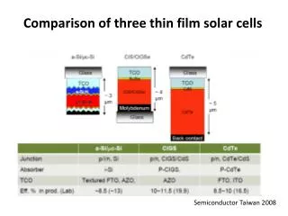
Nanocrystalline/microcrystalline based solar cells: a-Si/mc-Si module, 13.5% (4141 cm2 area)
Deposition of large area µc-Si films using PECVD 98% Hydrogen 95% Hydrogen
Raman spectra: Power= 100 Watt Power= 270 Watt
Effect of microstructure on the performance of single junction microcrystalline silicon solar cell
Silicon Quantum Dot Solar cell: • The ultimate objective is to enhance the efficiencies of solar cell by making use of quantum size effect. Quantum confinement occurs when size of the nanocrystals in a high bandgap dielectric matrix is comparable to the Bohr radius (~5 nm for Si) in bulk c-Si.
Fabrication of Si quantum dots • Quantum dots offer the potential to control the intermediate band energies. • Placing the appropriate quantum dot material of necessary size into an organized matrix in solar cell results in the formation of accessible energy levels . • Theoretically solar cells with quantum dots offer a potential efficiency of more than 40%.
Up to n layers Up to n layers SiOx SiO2 Annealed at 1000 oC SiO2 SiOx SiO2 SiO2 SiOx Substrate Substrate Schematic of superlattice structure • The SiOx/SiO2superlattice thickness depends on the thickness of each SiOx layer and SiO2 layer, and is also related to the number of periods (n)of the superlattice. In our case n = 50. The SiO2 layer was about 2 nm and thickness of the SiOx layer was varied from 3 to 7 nm. • The structure of the bilayer which consists of a SiOx and SiO2 is relaxed. At higher temperatures, the annealing of the amorphous SiOx films results in a phase separations described by: 2 SiOx x SiO2 + (2-x)Si (x changes from 0 to 2)
High resolution transmission electron microscopy SRSO films deposited at Y = 2.0 • In SRSO films nano crystalline silicon quantum dots of average size 5 – 8 nm surrounded by amorphous silicon oxide network have been observed.
Photoluminescence • Presence of visible PL peak at room temperature of SRSO materials can be explained by the quantum confinement effect theory. • PL band ~730 nm is due to nano-meter silicon grains embeded in SiOx network . • With increase of oxygen content oxygen rich region increases and number density of Si nanocrystals decreases. Thus the PL intensity decreases. 1. Co = 8.3 at% 2. Co = 9.3 at% 3. Co = 10.7 at%
Raman study of superlattice structure Quantum dot size was calculated from the formula: dRaman = 2π(B/ω) B= 2.0 cm-1; ω= peak shift for nc-Si:H compared to c-Si
Raman studies: Superlattice annealed at 900oC Superlattice annealed at 800oC • For the sample SL-1, annealed at 800oC, a-Si phase dominates and a weak signal of nc-Si has been detected near 515 cm-1. In SL-1, N2 is incorporated both in SiOx and SiO2 layer. • In case of SL-2 and SL-3 sharp peaks were observed indicating highly crystalline growth. In these two SL’s N2 has been incorporated only in SiO2 layers. In SL-3 SiOx sublayer thickness is 3 nm whereas it is 5 nm for SL-2.
X-ray diffraction studies: Superlattice annealed at 900oC Superlattice annealed at 800oC • When annealed at 800oC, SL-1 does not show any peak as N2 is incorporated in both SiOx and SiO2 sublayers. SL-2 and SL-3 have signature of <111>, <220> and <311> peaks of c-Si. When SL-1 was annealed at 900oC the three peaks with low intensity appeared.
High resolution transmission electron microscopy: Nanocrystalline silcons are formed in the amorphous silicon oxide layer with average size of 4 – 6 nm in diameter. SL-3 annealed 800oC SL-2 annealed 800oC SL-3 annealed 800oC SL-3 annealed 800oC SL-2 annealed 900oC SL-2 annealed 900oC SL-2 annealed 900oC SL-2 annealed 900oC
Fabrication of P-I-N Structure using a Si-QDSL Konagai et al fabricated the solar cells using Si-QDSL as a light absorption layer. From the I-V characteristics, the open circuit voltage and short circuit current were estimated to be 165 mV and 1.3 x 10⁻² mA/cm2. Later using N-containing Si-QDSL as an intrinsic layer and after passivation of interfaces Voc increased to 389mV and then 518mV.
n-type Si-QDSL/p-type c-Si photovoltaic device The best cell parameters obtained by Green et al were an open-circuit voltage Voc of 556 mV, short-circuit current Jsc of 29.8 mA/cm2, fill factor FF of 63.8 %, and conversion efficiency of 10.6 % from 3 nm Si-QDs with a 2 nm SiO2 layer.
The target structure of the all silicon tandem cell based on Si-QDSLs is as follows
Conclusions: • High efficiency can be realized using multijunction Si solar cell structure. • The electrical and optical properties of material change when the size of the crystal becomes less than the Bohr excitation radius. • SiOx/ SiO2 or SiyNx / Si3N4 superlattices can been developed by RFPECVD technique by varying the deposition conditions and annealing temperatures. • Presence of nanocrystals have been confirmed from Raman study, high resolution transmission electron microscopy and X-ray diffraction studies. • Ultimately the QDSL is a potential material for high efficiency low cost solar cell. To obtain high performance, extensive research work is needed and it will take sometime to realize high efficiency solar cell containing the third generation concepts.