Download
1 / 58
2.23k likes | 3.65k Views
ECE 404 PCB Design. By Julian Rene Cuellar Buritica. Guided by Dr. Scott Umbaugh Graduate Program Director Department of Electrical & Computer Engineering Southern Illinois University - Edwardsville. Overview. Introduction – Why PCB? Materials of PCB Parts of PCB Jumpers Solder Mask

E N D
ByJulian Rene Cuellar Buritica Guided by Dr. Scott Umbaugh Graduate Program Director Department of Electrical & Computer Engineering Southern Illinois University - Edwardsville
Overview • Introduction – Why PCB? • Materials of PCB • Parts of PCB • Jumpers • Solder Mask • Silkscreen • Multilayer PCB • Physical Design Issues • Design Software • Material Required to Design PCB • Manual PCB Design • PCB Manufacturing Companies
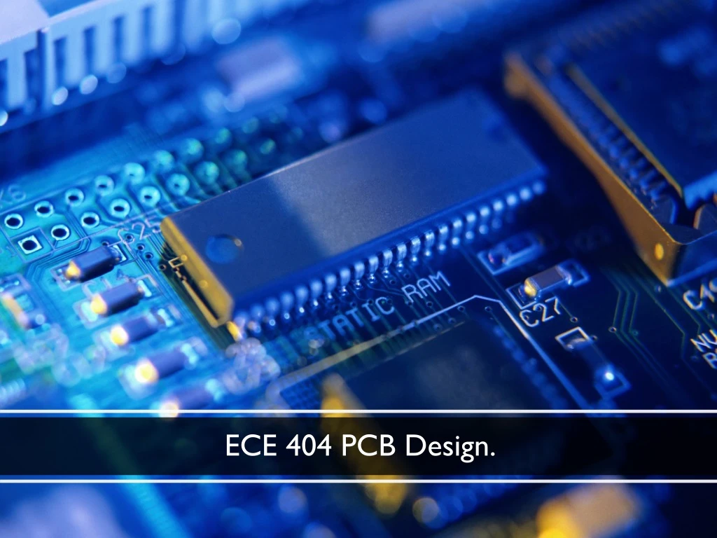
Introduction • Printed Circuit Board • Mechanical support • Electrically connect electronic components using conductive pathways, or traces • PCB populated with electronic components is a printed circuit assembly (PCA)
Why PCB? • Rugged, inexpensive, and can be highly reliable • Faster (due to automation) and consistent in high volume production • Professional(more neater look)
Materials of PCB • Conducting layers are typically made of thin copper foil. • The board is typically coated with a solder mask that is green in color. Other colors that are normally available are blue and red. • Unwanted copper is removed from the substrate after etching leaving only the desired copper traces or pathways
Dielectric PCB Layer • Most common material for PCB is the FR-4 board: • FR stands for Flame Retardant. • Composite material with woven fiberglass cloth with an epoxy resin binder. • Thickness of FR-4 and copper specified separately. • Copper foil thickness in (oz/ft^2), [simply ounce]. • 1 oz/ft^2 copper foil has a thickness of 35 µm. • 1/0 - 1 oz/ft^2 copper one side, with no on the other. • 1/1 - denotes 1 oz/ft^2 copper on both sides.
Parts of a PCB • Components • Pads • Traces • Vias • Top Metal Layer • Bottom Metal Layer
Components • Components are the actual devices used in the circuit. • This includes input/output connections. • I/O ports, including power supply connections, are also important in the PCB design.
Pads • Location that components connect to. • You will solder components to the pads on the PCB. • Pads will connect to traces. • Pads have an inner diameter and outer diameter.
Traces • Traces connect pads together. • Traces are essentially the wiring of the PCB. • Equivalent to wire for conducting signals • Traces sometimes connect to vias. • High current traces should be wide. • Signal traces usually narrower than power or ground traces
Vias • Pad with a plated hole connecting traces from one layer of board to other layers. • Attempt to minimize via use in your PCBs. • Some component leads can be used as vias.
Vias • Blind Via • Buried Via • Through hole Via
Top Metal Layer • Most of the components reside on the top layer • Fewer traces on the top layer • Components are soldered to the pads on the top layer of PCB • Higher circuit densities
Bottom Metal Layer • Few components on this layer. • Many traces on this layer. • Most soldering done on this layer.
Jumpers • Often, many signal wires need to exist in too small of a space and must overlap. • Running traces on different PCB layers is an option. • Multilayer PCBs are often expensive. • Solution: Use jumpers
Solder Mask • Protect copper traces on outer layers from corrosion • Areas that shouldn't be soldered may be covered with polymer resist solder mask coating • Designed to keep solder only in certain areas • Prevents solder form binding between conductors and thereby creating short circuits(i.e. hides traces from solder)
Soldering • Wave Soldering- for through hole and SMT • Reflow Soldering- for SMT
Silkscreen • Printing on the solder mask to designate component locations • Readable information about component part numbers and placement. • Helpful in assembling, testing and servicing the circuit board.
Multilayer PCBs • More than a top and bottom layer. • Typically there will be a power plane, ground plane, top layer, and bottom layer. • Sometimes signal layers are added as needed. • Sometimes RF planes made of more expensive materials are added.
Physical Design Issues • Component Size • Heat Dissipation • Input and Output • Mounting Points
Component Size • Make sure components will actually fit. • This especially applies for circuits that require high component densities. • Some components come in multiple sizes. SMT vs Through Hole • Sometimes you can get tall and narrow caps or short and wide capacitors.
Heat Dissipation-Heat Sinks • Heat sink dissipates heat off the component • Does not remove heat, just moves it • Some components get hot, requiring heat sink • Data sheets specify the size of the heat sink • A short circuit may result when two devices share the same heat sink
Mounting Points • PCB needs to be mechanically secured • To chassis-consist of metal frame on which the circuit boards and other electronic components are mounted • To another PCB/socket on PCB • To attachments to a heatsink
Parasitics • High frequency circuits • Series Inductance • Shunt Capacitance • Inductive Coupling • Capacitive Coupling
Series Inductance • Not an issue for low frequency circuits(<10 Mhz) • Inductance of a trace may be significant • Power connections - add shunt capacitor to counter the series inductance of a long trace • Capacitor has a low AC impedance • A 100nF capacitor is often used along with a larger capacitor. 100 nF ceramics have very low impedance at higher frequencies.
Shunt Capacitance • Result of wide wires over a ground plane. • Limits speed of circuits, including digital circuits • Insignificant for low performance circuits • Capacitor from voltage to ground will minimize
Inductive Coupling • Transfer of energy from one circuit component to another through shared magnetic field • Change in current flow through one device induces current flow in other device • Current flow in one trace induces current in another trace • Minimize the long parallel runs of traces • Run traces perpendicular to each other
Capacitive Coupling • Transfer of energy in electrical network due to capacitance between circuit nodes • Minimizing long traces on adjacent layers will reduce capacitive coupling • Ground planes are run between the signals that might affect each other.
Pre-work • Thoroughly simulate your circuit-make sure the circuit worked in simulations • Thoroughly test the prototype-make sure the circuit worked on the bread board • Have all the data sheets handy for all components • Try various component configurations
Simulations • Important to simulate the circuits before building them • Allow margin for component tolerances • Avoid using precise components. e.g a PWM controller that requires exact 10 V DC to work and will fail if there is 10.01V • High performance circuits or SMT devices require PCBs and should be simulated extensively first
Transferring your design to a board • Direct Transfer using marker • "Press-N-Peel" sheets and Variations use of heat • Blender pen • Photolithography use of UV light
DesignSoftware • Proteus Profesional • CADSoft EAGLE • PCBWizard • OrCAD … Gerber files: Describe the images of a printed circuit board (copper layers, solder mask, legend, etc.) as well as the drilling and milling data, de facto standard used by industry to describe PCB images
Materials Required to make PCB • Drill machine. • Cloth Iron. • Laser Printer. • Photo paper / Glossy paper. • Gloves. • Ferric Chloride (Etching solution) • PCB board. • Black permanent Marker.
Manual PCB design Step 1: Take printout of PCB layout • Using laser printer & glossy paper • Mirror image Step 2: Cutting the copper plate
Steps in PCB design Step 3: Make it smooth • Rub the copper side • Removes top oxide layer and photo resist layer • Sanded surface allow image to stick better
Steps in PCB design Step 4: Printing Design layout to board • Method 1: Iron on glossy paper ( transfers the toner) • Method 2: Circuit by hand (using marker)
Steps in PCB design Step 5: Apply heat (Iron it !!) • Iron it image down to copper side • Apply little pressure for 10-15 min • Iron heat transfer toner to cooper plate CAUTION: Do not directly touch copper plate because it is very hot due to ironing.
Steps in PCB design Step 6: Peeling • Place printed plate in Luke warm water (10 min) • Remove the paper • Use black marker to dark lighted track
Steps in PCB design Step 7: Etching • Dissolve 2-3 tea spoon ferric chloride in water • Dip PCB in etching solution for 30 min • FeCl3 reacts with unmasked Cu and removes unwanted Cu • Cu + FeCl3 = CuCl3 + Fe