Download
1 / 21
220 likes | 547 Views
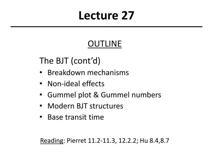
Lecture 27. OUTLINE The BJT (cont’d) Breakdown mechanisms Non-ideal effects Gummel plot & Gummel numbers Modern BJT structures Base transit time Reading : Pierret 11.2-11.3, 12.2.2; Hu 8.4,8.7. BJT Breakdown Mechanisms.

E N D
Lecture 27 OUTLINE The BJT (cont’d) • Breakdown mechanisms • Non-ideal effects • Gummel plot & Gummel numbers • Modern BJT structures • Base transit time Reading: Pierret 11.2-11.3, 12.2.2; Hu 8.4,8.7
BJT Breakdown Mechanisms • In the common-emitter configuration, for high output voltage VEC, the output current IC will increase rapidly due to one of two mechanisms: • punch-through • avalanche EE130/230A Fall 2013 Lecture 27, Slide 2 R. F. Pierret, Semiconductor Device Fundamentals, p. 409
Punch-Through E-B and E-B depletion regions in the base touch W = 0 As |VCB| increases, the potential barrier to hole injection decreases and hence IC increases EE130/230A Fall 2013 Lecture 27, Slide 3 R. F. Pierret, Semiconductor Device Fundamentals, Figs. 11.7-11.8
Avalanche Multiplication PNP BJT: • Holes are injected into the base [0], then collected by the B-C junction • Some holes in the B-C depletion region have enough energy to generate EHP [1] • Generated electrons are swept into the base [3], then injected into emitter [4] • Each injected electron results in the injection of IEp/IEn holes from the emitter into the base [0] • For each EHP created in the C-B depletion region by impact ionization, (IEp/IEn)+1 > bdc additional holes flow into the collector i.e. carrier multiplication in the C-B depletion region is internally amplified where VCB0 = reverse breakdown voltage of the C-B junction EE130/230A Fall 2013 Lecture 27, Slide 4 R. F. Pierret, Semiconductor Device Fundamentals, Fig. 11.9
Non-Ideal Effects at Low VEB • In the ideal transistor analysis, thermal R-G currents in the emitter and collector junctions were neglected. • Under active-mode operation with small VEB, the thermal recombination current is likely to be a dominant component of the base current • low emitter efficiency, hence lower gain This limits the application of the BJT for amplification at low voltages. EE130/230A Fall 2013 Lecture 27, Slide 5
Non-Ideal Effects at High VEB • Decrease in bdc at high IC is caused by: • high-level injection • series resistance • current crowding EE130/230A Fall 2013 Lecture 27, Slide 6
Gummel Plot and bdcvs.IC bdc bdc From top to bottom: VBC= 2V, 1V, 0V EE130/230A Fall 2013 Lecture 27, Slide 7 C. C. Hu, Modern Semiconductor Devices for Integrated Circuits, Figures 8-8 & 8-9
Gummel Numbers For a uniformly doped base with negligible band-gap narrowing, the base Gummel number is (total integrated “dose” (#/cm2) of majority carriers in the base, divided by DB) Emitter efficiency GE is the emitter Gummel number EE130/230A Fall 2013 Lecture 27, Slide 8
Notice that In practice, NB and NE are not uniform, i.e. they are functions of x The more general formulas for the Gummel numbers are EE130/230A Fall 2013 Lecture 27, Slide 9
Modern NPN BJT Structure • Features: • Narrow base • n+ poly-Si emitter • Self-aligned p+ poly-Si base contacts • Lightly-doped collector • Heavily-doped epitaxial subcollector • Shallow trenches and deep trenches filled with SiO2 for electrical isolation C. C. Hu, Modern Semiconductor Devices for Integrated Circuits, Figure 8-22 EE130/230A Fall 2013 Lecture 27, Slide 10
Poly-Si Emitter • bdcis larger for a poly-Si emitter BJT as compared with an all-crystalline emitter BJT, due to reduced dpE(x)/dx at the edge of the emitter depletion region Continuity of hole current in emitter: (1poly-Si; 2crystalline Si) EE130/230A Fall 2013 Lecture 27, Slide 11 R. F. Pierret, Semiconductor Device Fundamentals, Fig. 11-18
Emitter Gummel Number w/ Poly-Si Emitter where SpDEpoly/WEpoly is the surface recombination velocity For a uniformly doped emitter, EE130/230A Fall 2013 Lecture 27, Slide 12
Emitter Band Gap Narrowing To achieve large bdc, NE is typically very large, so that band gap narrowing is significant (ref. Lecture 3, Slide 20). DEGE is negligible for NE < 1E18/cm3 N = 1018 cm-3: DEG = 35 meV N = 1019 cm-3: DEG = 75 meV EE130/230A Fall 2013 Lecture 27, Slide 13
Narrow Band Gap (Si1-xGex) Base To improve bdc, we can increase niB by using a base material (Si1-xGex) that has a smaller band gap • for x = 0.2, DEGB is 0.1 eV This allows a large bdc to be achieved with large NB (even >NE), which is advantageous for • reducing base resistance • increasing Early voltage (VA) courtesy of J.D. Cressler (GATech) EE130/230A Fall 2013 Lecture 27, Slide 14
Heterojunction Bipolar Transistors • Uniform Ge concentration in base • Linearly graded Ge concentration in base built-in E-field EE130/230A Fall 2013 Lecture 27, Slide 15
Example: Emitter Band Gap Narrowing If DB = 3DE, WE = 3WB, NB = 1018 cm-3, and niB2 = ni2, find bdc for (a)NE = 1019 cm-3, (b)NE = 1020 cm-3, and (c)NE = 1019 cm-3 and a Si1-xGex base with DEGB = 60 meV (a) For NE = 1019 cm-3, DEGE 35 meV (b) For NE = 1020cm-3, DEgE 160 meV: (c) EE130/230A Fall 2013 Lecture 27, Slide 16
Charge Control Model A PNP BJT biased in the forward-active mode has excess minority-carrier charge QB stored in the quasi-neutral base: In steady state, EE130/230A Fall 2013 Lecture 27, Slide 17
Base Transit Time, tt • time required for minority carriers to diffuse across the base • sets the switching speed limit of the transistor EE130/230A Fall 2013 Lecture 27, Slide 18
Relationship between tB and tt • The time required for one minority carrier to recombine in the base is much longer than the time it takes for a minority carrier to cross the quasi-neutral base region. EE130/230A Fall 2013 Lecture 27, Slide 19
Built-in Base E-Field to Reducett The base transit time can be reduced by building into the base an electric field that aids the flow of minority carriers. 1. Fixed EGB, NB decreases from emitter to collector: B - E C Ec Ef Ev 2. Fixed NB, EGB decreases from emitter to collector: - E B C Ec Ef E Ev EE130/230A Fall 2013 Lecture 27, Slide 20
EXAMPLE: Drift Transistor • Given an npn BJT with W=0.1mm and NB=1017cm-3 (mn=800cm2/Vs), find tt and estimate the base electric field required to reduce tt EE130/230A Fall 2013 Lecture 27, Slide 21