Download
1 / 24
240 likes | 344 Views
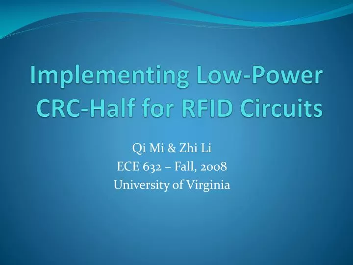
Implementing Low-Power CRC-Half for RFID Circuits. Qi Mi & Zhi Li ECE 632 – Fall, 2008 University of Virginia. Outline. Introduction Problem Statement Contribution Design Simulation Conclusion Future Work Q & A. Introduction. RFID applications RFID security issues.

E N D
Implementing Low-Power CRC-Half for RFID Circuits Qi Mi & Zhi Li ECE 632 – Fall, 2008 University of Virginia
Outline • Introduction • Problem Statement • Contribution • Design • Simulation • Conclusion • Future Work • Q & A
Introduction • RFID applications • RFID security issues
Problem Statement • Constraint: • Energy – foremost constraint • Size • Complexity • Problem: We seek to find a feasible way of implementing low-power data encryption on RFID tags.
Contribution • Implemented the core hash function (i.e., CRC-Half) of CRC-MAC with PTM 90nm technology. • Analyzed energy at different operating voltages. • Gave an optimal operating voltage point for CRC-MAC. • Analyzed the trend of leakage current of the circuit.
CRC-MAC Briefing Fig 1. A hardware implementation of CRC-MAC
CRC-MAC Briefing (cont’d) Fig 2. C implementation of CRC-MAC as keyed one-way function
Circuit Design Fig 3. A symbol view of CRC-Half
Optimization Design • Metric: Total energy consumption E/op = Eactive + Eleakage = CeffVDD2+ IlkgVDDTD • Knobs • Lower VDD (subthreshold design) Robust, require CMOS • Shorten operation duration
Simulation • Technology: PTM 90nm Technology • Circuit Description: netlists • Simulation Environment • Schematic-level • Software: FPGA Advantage 7.0 LS • Circuit-level • Software: Cadence 2005 • Simulator: Ocean with Spectre
Simulation (cont’d) • Approach
Spectre Simulation Result 1 0 1 1 Data word: 0010 1001 0010 1101 Key word: 1101 0010 0001 0111 Output: 1011 0001 0001 0111
Leakage Current Simulation Exponential Reduction as VDD decreases due to DIBL effect Leakage Current is independent of CLK rate
Current Waveform in One Cycle Pavg = α0→1fCeffVDD2 A higher CLK rate helps reduce energy consumption for a certain VDD
Energy Consumption Plot • The optimal supply voltage is around 0.3V • Leakage energy consumption starts to dominate in the sub-threshold region • Leakage current is taking up a large proportion of average current
Conclusion • CRC-processing circuit is simulated in FPGA and Cadence • Average and leakage currents are simulated • Energy consumption comparison for different VDD and VDD optimization for minimum energy consumption
Future Work • Use multiple power supplies to speed up the critical path • Size up some parts of the circuit to increase speed • Add high VT NMOS to the PDN to reduce leakage