Download
1 / 31
330 likes | 413 Views
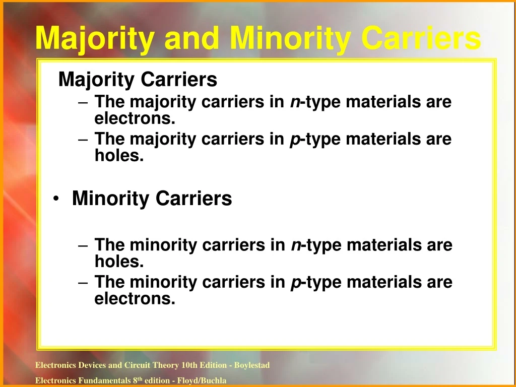
Majority Carriers The majority carriers in n -type materials are electrons. The majority carriers in p -type materials are holes. Minority Carriers The minority carriers in n -type materials are holes. The minority carriers in p -type materials are electrons.

E N D
Majority Carriers The majority carriers in n-type materials are electrons. The majority carriers in p-type materials are holes. Minority Carriers The minority carriers in n-type materials are holes. The minority carriers in p-type materials are electrons. Majority and Minority Carriers
One end of a silicon or germanium crystal can be doped as a p-type material and the other end as an n-type material. The result is a p-n junction. p-n Junctions
The result is the formation of a depletion region around the junction. p-n Junction
The diode is a 2-terminal device. Diodes A diode ideally conducts in only one direction.
A diode has three operating conditions: No bias Forward bias Reverse bias Diode Operating Conditions
No Bias No external voltage is applied: VD = 0 V No current is flowing: ID = 0 A Only a modest depletion region exists Diode Operating Conditions
Reverse Bias External voltage is applied across the p-n junction in the opposite polarity of the p- and n-type materials. Diode Operating Conditions
Reverse Bias Diode Operating Conditions The reverse voltage causes the depletion region to widen. The electrons in the n-type material are attracted toward the positive terminal of the voltage source. The holes in the p-type material are attracted toward the negative terminal of the voltage source.
Forward Bias External voltage is applied across the p-n junction in the same polarity as the p- and n-type materials. Diode Operating Conditions
Forward Bias Diode Operating Conditions
Conduction Non-Conduction Region Region Diode Characteristics
Zener diode Light-emitting diode Diode arrays Other Types of Diodes