Slide Note
0 likes | 7 Views
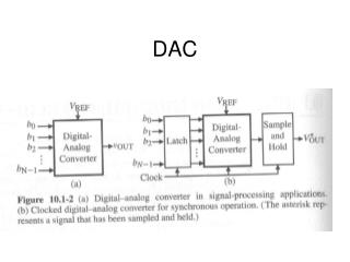
Learn how to interface analog-to-digital converter (ADC) chips like ADC0804, ADC0808/0809, ADC0848, and MAX1112 with the 8051 microcontroller. Understand the process of data acquisition, factors in selecting ADC chips, and programming ADC chips in C and Assembly language. Explore digital-to-analog converter (DAC) chips, interface a DAC chip with the 8051, and program it to generate a sine wave. Discover sensor interfacing, signal conditioning, and the role of precision IC temperature sensors in data acquisition.

E N D
THE 8051 MICROCONTROLLER & Embedded Systems Muhammad Ali Mazidi, Janice Mazidi & Rolin McKinlay
ADC, DAC, AND SENSOR INTERFACING Chapter 13
Objectives Upon completion of this chapter, you will be able to: >> >> >> >> >> >> >> >> >> >> >> >> >> >> Interface ADC (analog-to-digital converter) chips to the 8051 Interface temperature sensors to the 8051 Explain the process of data acquisition using ADC chips Describe factors to consider in selecting an ADC chip Describe the function of the pins of 804/809/848 ADC chips Describe the function of the pins of the MAX1112 serial ADC chip Interface serial ADC chips to the 8051 Program serial and parallel ADC chips in 8051 C and Assembly Describe the basic operation of a DAC (digital-to-analog converter) chip Interface a DAC chip to the 8051 Program a DAC chip to produce a sine wave on an oscilloscope Program DAC chips in 8051 C and Assembly Explain the function of precision IC temperature sensors Describe signal conditioning and its role in data acquisition
Objectives • More real-world devices such as ADCs (analog-to-digital converters), DACs (digital-to-analog converters), and sensors, and how to interface the 8051 to these devices, Section 13.1, analog-to-digital converter (ADC) chips, the 8-bit parallel ADC chips ADC0804, ADC0808/0809, and ADC0848 We will also look at the serial ADC chip MAX1112, Section 13.2, the characteristics of DAC chips Section 13.3, the interfacing of sensors and discuss the issue of signal conditioning • • •
Table 13-1: Resolution vs. Step Size for ADC n-bit 8 10 12 16 Notes: VCC= 5 V Step size (resolution) is the smallest change that can be discerned by an ADC. Number of steps 256 1024 4096 65536 Step Size (mV) 5/256 = 19.53 5/1024 = 4.88 5/4096 = 1.2 5/65536 = 0.076
Figure 13-1. ADC0804 Chip (testing ADC0804 in free running mode)
Figure 13-4. 8051 Connection to ADC0804 with Clock from XTAL2 of the 8051
Table 13-3: ADC0808/0809 Analog Channel Selection Selected Analog Channel IN0 IN1 IN2 IN3 IN4 IN5 IN6 C 0 0 0 0 1 1 1 B 0 0 1 1 0 0 1 A 0 1 0 1 0 1 0
Figure 13-6. Selecting a Channel and Read Timing for ADC0809
Figure 13-8. ADC0848 Chip Table 13-5: ADC0848 Vrefvs. Step Size
Example 13-1 For a given ADC0848, we have Vref = 2.56 V. Calculate the D0 - D7 output if the analog input is: (a) 1.7 V, and (b) 2.1 V. Solution: Since the step size is 2.56/256 = 10 mV, we have the following. (a) Dout = 1.7 V/10 mV = 170 in decimal, which gives us 10101011 in binary for D7 - D0. (b) Dout = 2.1 V/10 mV = 210 in decimal, which gives us 11010010 in binary for D7 -D0. SJMP AGAIN ;keep sending A
Table 13-6: ADC0848 Analog Channel Selection (Single-Ended Mode)
Figure 13-10. Selecting a Channel and Read Timing for the ADC0848
Figure 13-12. MAX1112 Chip Figure 13-13. MAX1112 Serial ADC Block Diagram
Figure 13-14. MAX1112 Control Byte Start The MSB (D7) must be high to define the beginning of the control byte. It must be sent in first. SEL1 SEL0 CHANNEL SELECTION (SINGLE-ENDED MODE) 0 0 CHAN0 0 1 CHAN1 1 0 CHAN2 1 1 CHAN3 0 0 CHAN4 0 1 CHAN5 1 0 CHAN6 1 1 CHAN7 SEL2 0 0 0 0 1 1 1 1 UNI/BIP 1 = unipolar: Digital data output is binary 00 - FFH. 0 = bipolar: Digital data output is in 2’s complement. 1 = single-ended: 8 channels of single-ended with COM as reference 0 = differential: Two channels (eg., CH0 - CH1) are differential. 1 = fully operational 0 = power-down: Power down to save power using software. 1 = external clock mode: The conversion speed is dictated by SCLK. 0 = internal clock mode: The conversion speed is dictated internally, and the SSTRB pin goes high to indicate end-of-conversion (EOC). SGL/DIF PD1 PD0
Example 13-2 Find the MAX1112 control byte for (a) CH0, (b) and (b) CH3. Assume single-ended, unipolar, internal clock, and fully operational modes. Solution: From Figure 13-14, we have the following: (a) 10001110 (8E in hex) (b) (b) 10111110 (BE in hex)
Example 13-3 Assuming that R = 5K and Iref= 2 mA, calculate Voutfor the following binary inputs: (a) 10011001 binary (99H) (b) 11001000 (C8H) Solution: (a) Iout= 2 mA (153/256) = 1.195 mA and Vout= 1.195 mA x 5K = 5.975 V (b) Iout= 2 mA (200/256) = 1.562 mA and Vout= 1.562 mA x 5K = 7.8125 V
Example 13-4 In order to generate a stair-step ramp, set up the circuit in Figure 13-18 and connect the output to an oscilloscope. Then write a program to send data to the DAC to generate a stair-step ramp. Solution: CLR MOV INC ACALL SJMP A P1,A A DELAY AGAIN AGAIN: ;send data to DAC ;count from 0 to FFH ;let DAC recover
Example 13-5 Verify the values given for the following angles: (a) 30° (b) 60°. Solution: (a) Vout= 5 V + (5 V x sin q) = 5 V + 5 x sin 30° = 5 V + 5 x 0.5 = 7.5 V DAC input values = 7.5 V x 25.6 = 192 (decimal) (b) Vout= 5 V + (5 V x sin q) = 5 V + 5 x sin 60° = 5 V + 5 x 0.866 = 9.33 V DAC input values = 9.33 V x 25.6 = 238 (decimal)
Figure 13-20. Getting Data From the Analog World Table 13-11: Temperature vs. Vout for ADC0848
Figure 13-21. 8051 Connection to ADC0848 and Temperature Sensor