Download
1 / 32
320 likes | 412 Views
Circuit-wise Buffer Insertion and Gate Sizing Algorithm with Scalability. Zhanyuan Jiang and Weiping Shi. DAC 2008, June 8–13, 2008, Anaheim, California, USA. Outline. Introduction Problem Formulation Algorithm Post-buffering Timing Estimation

E N D
Circuit-wise Buffer Insertion and Gate Sizing Algorithm with Scalability Zhanyuan Jiangand Weiping Shi DAC 2008, June 8–13, 2008, Anaheim, California, USA.
Outline • Introduction • Problem Formulation • Algorithm • Post-buffering Timing Estimation • Linear Modeling of Non-linear Delay vs. Cost Tradeoff • Dynamic Critical Sink Selection • Linear Programming • Circuit Partition • Experimental Results • Conclusion
Outline • Introduction • Problem Formulation • Algorithm • Post-buffering Timing Estimation • Linear Modeling of Non-linear Delay vs. Cost Tradeoff • Dynamic Critical Sink Selection • Linear Programming • Circuit Partition • Experimental Results • Conclusion
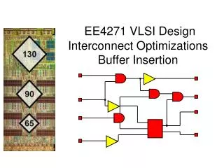
Introduction • As VLSI technology enters the nanoscale regime, a great amount of efforts have been made for timing optimization. • Among them, buffer insertion stands out as an effective technique to reduce interconnect delay. • Due to technology shrinking, more and more gates are placed on a chip, and algorithms without scalability can not fit into future physical synthesis flow.
Outline • Introduction • Problem Formulation • Algorithm • Post-buffering Timing Estimation • Linear Modeling of Non-linear Delay vs. Cost Tradeoff • Dynamic Critical Sink Selection • Linear Programming • Circuit Partition • Experimental Results • Conclusion
Problem Formulation • We represent a combinational circuit as a Directed Acyclic Graph (DAG) G = (V,E).
Problem Formulation • The paper abstract the routing tree of the circuit and ignore all the details (i.e., Steiner node and interconnect tree structure, etc.) within the routing tree. • The vertices only represent PI/PO of the circuit and input/output pins of modules while edges only for input-to-output paths within a module.
Outline • Introduction • Problem Formulation • Algorithm • Post-buffering Timing Estimation • Linear Modeling of Non-linear Delay vs. Cost Tradeoff • Dynamic Critical Sink Selection • Linear Programming • Circuit Partition • Experimental Results • Conclusion
Post-buffering Timing Estimation • A post-buffering timing estimation technique is proposed in [12], which derives delay equations along a buffered wire segment and applies the equations for the delay estimation upon multiple-sink nets.
Linear Modeling of Non-linear Delay vs. Cost Tradeoff • Table 1 shows that the impact of varying downstream sink size from 1X to 4X is negligible at the driver.
Linear Modeling of Non-linear Delay vs. Cost Tradeoff • A curve fitting method is adopted to approximate each tradeoff as several linear segments. • In this paper, the number of segments is set as 2, which gives good accuracy. ( If the number of segments is 3, the final circuit Elmore delay improves less than 0.1% while the linear programming solver time increases more than 50%. )
Linear Modeling of Non-linear Delay vs. Cost Tradeoff Qroot + c1Xc + c3 ≤ Qsink, (1) Qroot + c2Xc + c4 ≤ Qsink, (2) Lc ≤ Xc ≤ Uc, (3) Qroot :RAT values at root Qsink :RAT values at sink Xc :the number of buffers at this net Ci :the curve fitting coefficient Lc, Uc :lower bound and upper bound of the number of buffers
Dynamic Critical Sink Selection • A multiple-sink net contains sink S1, S2, · · · , Sn, and each sink has corresponding RAT Q1, Q2, · · · , Qn. It is hard to know which is critical sink before the stage of buffer insertion. • At the root, for a specific buffer number, we select the solution that minimizes the maximum delay among all sinks. Thus, only one delay cost tradeoff curve is returned.
Dynamic Critical Sink Selection Solution set 1 Solution set 2
Dynamic Critical Sink Selection Qroot + c1Xc + c5 ≤ Qsinkone, (1) Qroot + c2Xc + c6 ≤ Qsinkone, (2) Qroot + c3Xc + c7 ≤ Qsinktwo, (3) Qroot + c4Xc + c8 ≤ Qsinktwo, (4) Lc ≤ Xc ≤ Uc, (5) Qroot :RAT values at root Qsink :RAT values at sink Xc :the number of buffers at this net Ci :the curve fitting coefficient Lc, Uc :lower bound and upper bound of the number of buffers
Linear Programming Ci :the curve fitting coefficient Xi :the cost of routing tree RT(i) Lc, Uc :lower bound and upper bound
Circuit Partition • This paper adopt the divide-and-conquer scheme to speed up the algorithm. • The key components of the circuit partition technique are how to decide partition boundaries and how to set up side inputs/outputs in the sub-circuits.
Circuit Partition • In order to minimize partition error, the technique avoids partitioning the critical paths into different sub-circuits, which means that partition boundaries never cut through the most critical path. • If there is an overlap between different downstream cones, the overlap part belongs to the cone with the most critical primary input.
Circuit Partition Figure 5: The circuit is partitioned into three subcircuits based on the downstream cones of primary inputs. The input a is the most critical primary input in the circuit.
Outline • Introduction • Problem Formulation • Algorithm • Post-buffering Timing Estimation • Linear Modeling of Non-linear Delay vs. Cost Tradeoff • Dynamic Critical Sink Selection • Linear Programming • Circuit Partition • Experimental Results • Conclusion
Outline • Introduction • Problem Formulation • Algorithm • Post-buffering Timing Estimation • Linear Modeling of Non-linear Delay vs. Cost Tradeoff • Dynamic Critical Sink Selection • Linear Programming • Circuit Partition • Experimental Results • Conclusion
Conclusion • Experiments demonstrate that the circuit-wise algorithm achieves on average 17.4X speedup compared with the path based algorithm.
The whole circuit is partitioned into n downstream cones plus the remaining circuit. • The circuit is partitioned into n + m or n + k sub-circuits depending on whether the remaining circuit is disjointed or not.
The problem defined as follows: • Given a DAG which represents a placed and routed combinational circuit, possible candidate buffer locations, a buffer library and a gate library, find a buffering and gate sizing solution such that the total cost of buffers and gates are minimized, and the required arrival time at each primary input is less than a given constant constraint.
Elmore delay D(e) =R(e)[C(e)/2 + C(vj)] D(vj) = K(b) + R(b) .C(vj) e: edge (vi, vj) R(e): resistance of e C(e): capacitance of e C(vj): downstream capacitance at vj K(b): intrinsic delay of buffer b R(b): driving resistance of buffer b