Download
1 / 8
80 likes | 194 Views
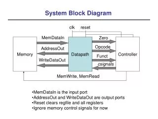
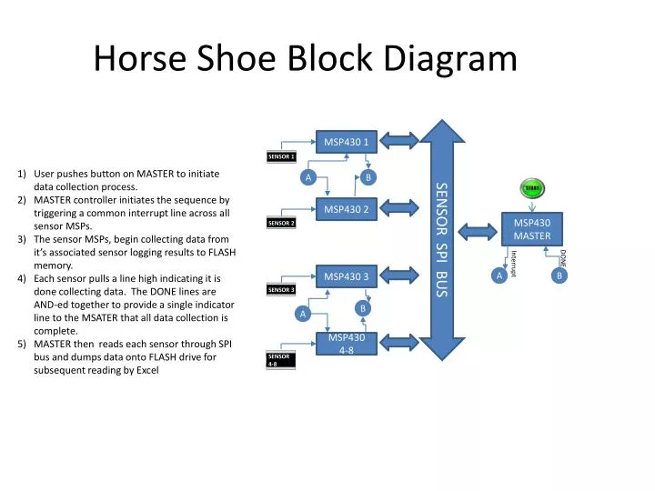
SENSOR SPI BUS. MSP430 1. Horse Shoe Block Diagram. User pushes button on MASTER to initiate data collection process. MASTER controller initiates the sequence by triggering a common interrupt line across all sensor MSPs.

E N D
SENSOR SPI BUS MSP430 1 Horse Shoe Block Diagram User pushes button on MASTER to initiate data collection process. MASTER controller initiates the sequence by triggering a common interrupt line across all sensor MSPs. The sensor MSPs, begin collecting data from it’s associated sensor logging results to FLASH memory. Each sensor pulls a line high indicating it is done collecting data. The DONE lines are AND-ed together to provide a single indicator line to the MSATER that all data collection is complete. MASTER then reads each sensor through SPI bus and dumps data onto FLASH drive for subsequent reading by Excel SENSOR 1 A B MSP430 2 MSP430 MASTER SENSOR 2 DONE Interrupt MSP430 3 A B B SENSOR 3 A MSP430 4-8 SENSOR 4-8
Memory Map 0x0000 Peripherals 512 Bytes 0x01FF 0x0200 128 Bytes RAM 0x027F 0x103F 0x1000 SEGMENT D Information 0x107F 0x1040 SEGMENT C 0x10BF SEGMENT B 0x1080 256 Bytes 0x10FF 0x10C0 SEGMENT A 0xF800 Your Program starts loading here SEGMENT 3 0xFA00 SEGMENT 2 1,983 Bytes Main 0xFC00 SEGMENT 1 0xFE00 0xFFCF SEGMENT 0 0xFFC0 Interrupts 64 Bytes (Block 0-7) 0xFFFF
Memory MapSensor (Slave) Storage 0x0000 Peripherals 512 Bytes 0x01FF 0x0200 128 Bytes RAM 0x027F • Sensors (Slave MSPs) store ADC results in a few different locations (segments) in FLASH memory. • The program performs 704 ADC reads of the sensors at 8-bit resolution. The results are stored in the following locations in FLASH memory: • Segment 1 of Main Memory (512 bytes) • Segment D of Information Memory (64 Bytes) • Segment C of Information Memory (64 Bytes) • Segment B of Information Memory (64 Bytes) • Total 704 Bytes 0x103F 0x1000 SEGMENT D Information 0x107F 0x1040 SEGMENT C 0x10BF SEGMENT B 0x1080 256 Bytes 0x10FF 0x10C0 SEGMENT A 0xF800 Your Program starts loading here SEGMENT 3 0xFA00 SEGMENT 2 1,983 Bytes Main 0xFC00 SEGMENT 1 0xFE00 0xFFCF SEGMENT 0 0xFFC0 Interrupts 64 Bytes (Block 0-7) 0xFFFF
Horse Shoe ADC Sensor Samples • Total 250 Samples • 25 Samples/Second • Over 10 Second period • Each sample requires 3 Bytes • 10 bit ADC (2 Bytes) • Sequence number (1 Byte) • Total Storage required 250*3=750 Bytes FLASH Memory ADC (2 Bytes), Sequence # (1 Byte) ADC (2 Bytes), Sequence # (1 Byte) ADC (2 Bytes), Sequence # (1 Byte) ADC (2 Bytes), Sequence # (1 Byte) ADC (2 Bytes), Sequence # (1 Byte) ADC (2 Bytes), Sequence # (1 Byte) ADC (2 Bytes), Sequence # (1 Byte) ADC (2 Bytes), Sequence # (1 Byte) ADC (2 Bytes), Sequence # (1 Byte) ADC (2 Bytes), Sequence # (1 Byte) ADC (2 Bytes), Sequence # (1 Byte) ADC (2 Bytes), Sequence # (1 Byte) ADC (2 Bytes), Sequence # (1 Byte) ADC (2 Bytes), Sequence # (1 Byte) ADC (2 Bytes), Sequence # (1 Byte) ADC (2 Bytes), Sequence # (1 Byte) ADC (2 Bytes), Sequence # (1 Byte) ADC (2 Bytes), Sequence # (1 Byte) ADC (2 Bytes), Sequence # (1 Byte) ADC (2 Bytes), Sequence # (1 Byte) ADC (2 Bytes), Sequence # (1 Byte) ADC (2 Bytes), Sequence # (1 Byte) ADC (2 Bytes), Sequence # (1 Byte) ADC (2 Bytes), Sequence # (1 Byte) ADC (2 Bytes), Sequence # (1 Byte) 1 2 3 4 5 6 7 8 9 10 11 12 13 14 15 16 17 18 19 20 21 22 23 24 25 1 Second
Program Sequence User Pushes Button START Interrupt Master MSP430 Erase Thumb Drive Wait for ALL DONE indicator from Salve MSPs SLAVE 1 EACH SLAVE Put Address for 1st slave on Address Bus SLAVE 2 Wait for /CS Erase FLASH SLAVE 3 SPI Read Slave Data SLAVE n Pause 1 Second SPI Data From FLASH to MASTER Write Slave Data to Thumb Drive 8 times Read ADC END Next Slave Pause 1/30th Second 250 times Close Thumb Drive Store ADC Reading & Sequence # in FLASH END Indicate Done
DONE Signal • After the Interrupt signal is received (when the user presses the start button) • The Slave MSP430s start to collect & store sensor data • When they are finished they send back a DONE signal to the Master MSP430, • When the Master has received the DONE signal indicating ALL of the Slaves have completed their data collection, then Master can start the phase where Master collects the data from each Slave • To save Chip-count & cost • The Slaves’ DONE signals are cascaded • Slave 8 signals DONE to Slave 7 • After Slave 7 completes it’s data collection AND receives a DONE signal from Slave 8, Slave 7 signals DONE to Slave 6 • And so on until all Slaves are DONE • Slave 1 signals DONE to Master indicating that ALL Slaves are DONE MASTER DONE SLAVE 1 DONE SLAVE 2 DONE SLAVE 3 DONE SLAVE n
Horse Shoe Block Diagram SENSOR 1 SENSOR 8 SENSOR 7 SENSOR 2 SENSOR 6 SENSOR 3 SENSOR 4 SENSOR 5
Flowchart User Pushes Button Sends Interrupt to Master & Salves Salves Pause for 1 second, Read & store data Master waits until it received READY signal from all Slaves Salves send READY signal to Master Salves send Data to Master when asked Master reads each Slaves data one at a time, storing results in FLASH Drive