Download
1 / 43
490 likes | 774 Views
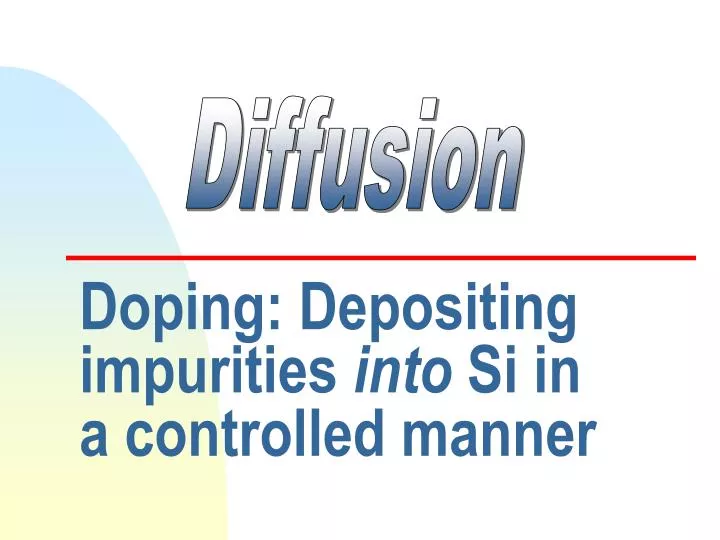
Doping: Depositing impurities into Si in a controlled manner. Diffusion. Overview. Diffusion vs Implantation Mechanism,Models Steps Equipment. Goal:. Controlled Junction Depth Controlled dopant concentration and profile.

E N D
Doping: Depositing impurities into Si in a controlled manner Diffusion
Overview • Diffusion vs Implantation • Mechanism,Models • Steps • Equipment
Goal: • Controlled Junction Depth • Controlled dopant concentration and profile Preferred location of maximum concentration need not be the surface P+ P+ Drain Source N “well” Wafer (Substrate): P Type
Electric Field Ions Diffusion & Ion Implanatation Ion Implantation Bombardment of ions SOURCE • Junction is where N = P • Can also be used when doping N in N OXIDE BLOCK Wafer (Substrate)`
Diffusion OXIDE BLOCK Diffusion & Ion Implantation • Diffusion • Solid-in-solid • high temperatures (1000 C) • Distances covered are in um or nm Wafer (Substrate)`
Mechanism , Models • Substitutional (10-12 cm2/s) • Interstitial replacement (10-6 cm2/s) • Interstitial movement • Substitutional preferred (better control) • Au, Cu diffuse by interstitial mechanism • B, P etc by substitutional mechanism • Two ideal cases • Constant source, limited source • Using Fick’s First & second law • J = Flux • D - Diffusivity of A in B • N- Concentration • x - distance
Models • Limited source • Dose Q = constant • Approx by Delta Fn • Constant Source • Concentration at x=0 is No • Complementary Error Function • Total Dose Q
Models • Constant Source • Concentration at x=0 is No Important Parameter : Dt species, temp and time N0 Impurity Concentration 3 2 1 Distance from Surface
Models • Limited Source • Dose Q Important Parameter : Dt N0 Area under the curve is constant If you normalize, erfc drops faster than Gaussian Impurity Concentration 3 1 2 Distance from Surface
Diffusivity • Diffusivity • Follows Arrhenius behavior • Wafer goes through heating cycles many times in the process • Effective Diffusivity * time = sum (Diffusivity * time) • Concept of thermal budget
Diffusion • Max absorption (at a given temp) • Usually quite high • Good for emitter and collector, but not for base • Not all dopant can contribute to electron/hole near solubility limit • Solubility limit in the range of 10 20/cm3 at 1000o C • Diffusion into silicon • Faster on grain boundaries • 10 times in poly silicon • Diffusivity in SiO2 usually very low (Segregation occurs)
Junction Formation N Carrier Conc Impurity Conc P Jn Distance from surface
OXIDATION Dopant Diffusion Diffusion: Drive In: Dopant re distribution • Deposited dopant must be pushed into Si • Re-distribution of dopant • Oxidation of exposed Si to protect *Dopant profile changes due to diffusion * Also due to preference for Oxide/Silicon: N-type piles up in Si, P-type depletes in Si
Diffusion • 1.Pre Clean • To remove particles • Thin oxide grows Dep OXIDE BLOCK Diffusion: Steps • 2.HF Etch • To remove oxide • Not too much! • 3.Deposit (pre dep) • Deposit enough to be higher than the solubility limit • 4.Drive In • High temp to enable diffusion inside Si • Also forms SiO2 (with high dopant concentration) • 2-STEP diffusion (usual) • 5.Deglaze (HF Etch) • Oxide may act as dopant source in future steps • Removing highly doped oxide may be problem (for dry etch)
Diffusion: Dep: schematic Wafers are Horizontal Gas Flow Better Uniformity Less wafers per batch Vertical Poor Uniformity More wafers per batch (or can have smaller chamber) Gas Flow Dummy wafers placed in the beginning & end
Doping: Gas phase • Dopant can be in Gas/Liquid/Solid state, but is typically carried using N2 in gaseous form • *Carrier gas may be bubbled through liquid source • *Carrier gas may pass over heated solid source • * inert gas can provide volume to maintain laminar flow Chamber Carrier Gas (N2) + Source Reaction gas
Phosphorus oxy chloride Phosphine Arsenic Oxide Diborane Boron Tribromide Reaction/Diffusion Limited Doping: Gas phase
Solid phase • Solid Source • Slugs between wafers • Lower through put • Cleaning is issue (slugs can break) • Safer to handle(no toxic vapor at room temp) • Spin coating (with solvents) • Similar to photo resist coating • Cost of extra spin/bake steps • thickness variations
Phosphorous pentoxide Arsenic Oxide Antimony Tri Oxide Boron Trioxide Tri Methyl Borate (TMB) Doping: Solid phase
Issues • Side diffusion • Increases with temperature/time • Limits the space between devices • Maximum dopant concentration is near surface • ==> majority of current near surface • (Surface tends to have max defects) • ==> less control • Dislocation generation (thermal drive in) • Surface contamination (dep) • Low dopant concentration and thin junction (small junction depth) are difficult At 0.18 um , junction depth is ~ 40 nm At 0.09 um, junction depth may be 20 nm
BLOCK Diffusion OXIDE BLOCK Issues: Side diffusion Side diffusion (Lateral Diffusion) Wafer (Substrate)`
Example of Real systems : *Hitachi-Zestone VII *2m x 3m x 3m *300 mm wafer *one wafer at a time * lower thermal budget, * better control, uniformity * low throughput *Hitachi-Vertron V *1m x 3.5m x 3.3m *200 mm wafer *150 wafers at a time * higher thermal budget, * good control, uniformity * high throughput
Gettering • To remove unwanted impurities • Try to get them to the back of wafer • Defects • Ar implant • Dep SiN/SiO2 (stress) • Oxygen during crystal growth (intrinsic) • High Conc P on back of wafer
Measurement • Sheet Resistance (average) • Four point probe, VDP (Van der Pauw) • Bevel • Interference • Dye • SIMS
Diffusion: Summary • Diffusion • Temp, Time, Thermal budget • Doping (more important for older nodes) • Relevant for all nodes • 2 step (constant source, limited source) • Solid/Liq/Gas
Ion Implantation • “Somewhat similar” to Sputtering • Dopant goes inside the silicon • sputtering deposits on the surface • Used for controlled doping • concentration • profile (depth) • Equipment • Mechanism • Issues • Summary
Equipment © Peter van Zant
1. Ion Source • Gas or solid source (no liquid source) • Solid heated to obtain vapor (P2O5) • effectively gas source • Mass flow meters (to control the flow better) • Gas usually Fluorine based • Ionization chamber • low pressure (milli/ micro torr) to ionize and minimize contamination • heated filament (thermionic emission) • positively charged ions created
2. Analyzing • Selection, analyzing, mass analyzing, ion separation • Similar to Mass Spectroscope • Usually the second stage (before acceleration) • Magnetic field to control the path • Charge to Mass Ratio • Some of the species from BF3 source • Selection of B+
3. Acceleration • Acceleration needed for implantation • Positive ions accelerated with ring anodes • Energy range: 5 keV for low, 2 MeV for high • Medium current : 1 mA • High current: 10 mA • Current ~ Dose • Beam Focus (magnetic/electric) SOI 100 mA High Current Oxygen • High energy ==> high throughput • few seconds per wafer 10 mA High Current Beam Current Low Energy High Energy Low Current 1 mA keV MeV Accln Energy
4. Scanning • Beam size ~ 1 sqr cm • Wafer size 200 mm or 300 mm • Issues: • neutral atoms need to be removed because... • dose calculated by current integrator • Electrical (beam) scanning & Mechanical (wafer) scanning • Beam Scan:(medium current) • beam moves outside the wafer for turn • controlling XY plates may be destroyed by discharge • Rotate wafer for uniformity • Wafer scan: (high current) • Beam shuttering: (electrical/mechanical) turn beam off when not on wafer
5. Target chamber • End chamber • low particle, high vacuum • Wafer held on • clamp (more particles) OR ESC (less particles) • Anti-static devices on the chamber • Integrate the current to measure dose • For 2+ ions, divide by 2 and so on... • Wafer charging: • minimize by connecting wafer to ground (with a charge counter) • dielectrics may get damaged • use flood gun to provide electron (and count it in measurement)
Electrons attract the +vely charged ions Nuclei repel the +vely charged ions Mechanism • Inelastic collision: • Electron (ionization) • Nuclear (nuclear reactions) • Elastic collision • Electron • Nuclear (atom substitution) • At low energy Nuclear collisions predominant • At high energy electronic collisions predominant • Variation in ‘stopping cross section’ • Gaussian profile expected (projected range Rp)
Implantation • Mask with Photoresist or oxide • resist for medium and low energy, moderate dose • high energy/high dose: increase in temp • Resist re-flow • Cross link (for organics) • less soluble (stripping an issue) • Faraday Cage • Retain secondary electron from wafer • Otherwise, wafer under dosed -Ve Bias e-
Gaussian OXIDE BLOCK Transverse Straggle (Diffraction) Issue: Transverse Straggle implant Even in implantation, dopants present in lateral direction
Channeling Some ions will move through “channels” without experiencing nuclear or electron collision for a “long” time ==> No Gaussian Profile
==> increase transverse straggle(called undercut) Also causes “shadow” Undercut Shadow Channeling 1. Hold the wafer at an angle (~ 8 degree) BLOCK ==> Too much angle is also a problem
OXIDE BLOCK Channeling 2. Dep amorphous material on the top It has to be very thin and not stop ions implant 3. Damage top of wafer and make it amorphous (eg high energy silicon implant)
Channeling 4. Increase temperature ==> reduce channel cross section Channeling critical angle ~ (Z/E) 1/2 ==> Low energy implants more likely to channel
TED • Transient Enhanced Diffusion • Damage during implantation • ==> point defects (vacancies) • interstitial silicon atoms • reduced during anneal • Channel dopant diffuse to surface • ==> VT modification ©Solid State Technology
RTA • Anneal to heal the damage • Diffusion during anneal an issue • High temp repair is faster than anneal • Repair energy barrier 5 eV, diffusion barrier 3 or 4 eV • 1. Adiabatic (laser, heats surface , < micro sec) • profile control difficult (not used) • 2. Thermal flux ( micro to 1 sec) • laser, ebeam, flash lamp • surface+bulk heating • rapid cooling ==> point defects • 3. Iso thermal (W-Halogen lamp) • 30 sec (1100 C)
Diffusion vs Ion Implantation Dep+Diffusion: depends on chemical nature and solubility Implantation: on energy of ion beam Expensive Better Control of junction depth, dose, profile Less ‘transverse straggle’