Download
1 / 29
290 likes | 407 Views
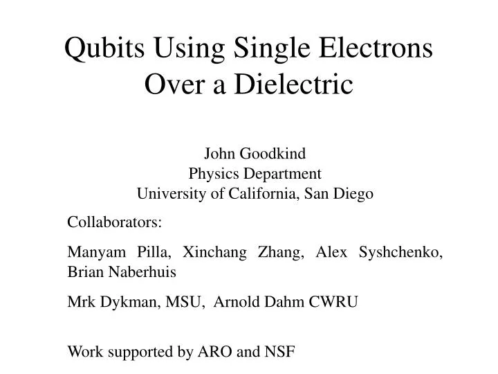
Qubits Using Single Electrons Over a Dielectric. John Goodkind Physics Department University of California, San Diego Collaborators: Manyam Pilla, Xinchang Zhang, Alex Syshchenko, Brian Naberhuis Mrk Dykman, MSU, Arnold Dahm CWRU Work supported by ARO and NSF.

E N D
Qubits Using Single Electrons Over a Dielectric John Goodkind Physics Department University of California, San Diego Collaborators: Manyam Pilla, Xinchang Zhang, Alex Syshchenko, Brian Naberhuis Mrk Dykman, MSU, Arnold Dahm CWRU Work supported by ARO and NSF
A clean physical system for qubits • The Hamiltonian for the system is well known and simple enough to be used to calculate the parameters required for logic operations • The interactions with the outside are also well known so that relaxation times can be estimated. • Swap and CNOT gates are easily implemented as a consequence of the interactions between qubits. The swap gate can be turned on and off by detuning specific qubits with the Stark shift. Refocusing can be used in exactly the same manner as for nmr qubits.
electron, in vacuum, above the surface of a dielectric, is attracted to that surface by the induced polarization. • The resulting electric field is from an image charge so that • Very close to the surface, the potential becomes strongly repulsive. • Application of an electric field yields a first order Stark shift.
In order to apply stark shifts to individual electrons, they must be confined laterally over a micro-electrode. d
Some properties of the system • qubits are coupled to electric fields so that they can be manipulated by easily obtainable DC and microwave fields • easy to detect 1 electron (compared to 1 spin) • qubits are coupled by Coulomb force • qubits are in vacuum, weakly interacting with rest of universe at operating T = 10 mK • It is fabricated by standard lithographic techniques
Thus the Schrodinger equation for the system of interest is that of a 1D hydrogen atom with a modified charge. For liquid helium =1.05723, =6.95510-3 For solid Neon = 1.24, = 0.0268
- L 2 2 e 2 h = = - y = - U zExp [ z / l ] 0 0 2 3 / 2 2 l 2 ml l æ ö 1 1 1 z y = - - 2 ç ÷ z z Exp [ ] 1 3 / 2 2 l 2 l è ø l 2 We will use the first two of these eigenstates as qubits. , U U , = /4 1 0 For liquid helium l = 7.64 nm, U1 – U0 ~ 118 GHz Confirmed by experimental measurements. For solid Neon l =1.98 nm, U2 – U1 = 2.1 THz. At this frequency optical techniques can be used
In order to change the state of the qubit we will apply a microwave pulse at frequency, W. This adds a time dependent potential to the Hamiltonian. If U1 - U0, this will cause transitions between states at the “Rabi” frequency. R 1 GHz per V/cm The time dependent problem can be solved by expanding the time dependent wave function in terms of the eigenstates of the time independent Hamiltonian and then using the interaction representation.
We write the expansion as The the coupled differential equations for the cn(t) are:
The confining force in the plane can be designed so that in plane resonance frequency is comparable to E2 – E1. The fields shown are for 1 Volt applied to the electrodes. In practice we can achieve > 20 GHz in plane resonance frequency so that transitions will be induced only between the same in plane states. Ez must be reduced to 400 V/cm over the electrodes. Can be done by superimposing a uniform field.
One qubit electron gates On resonance C2(0)=0 C1(0)=1 Red = real, green= imaginary
Detuning by Stark shift Potentials applied to the electrodes shift the energy level spacing as described above (about 1.4 GHz for 100 Volt/cm). Thus, if we use fixed microwave frequency individual electrons will be tuned into resonance by adjusting the DC potentials. This provides the ability to address individual qubits.
The interaction between qubits Logic operations require interactions between qubits and for this case it is due to the Coulomb field of the electrons. d = 500 nm and <(z1 – z2)> between the first excited state and the ground state for helium is 34.4 nm. Expand and keep only first order terms.
The last term leads to a SWAP operation when two qubits are in resonance. This interaction also leads to an electric field from one electron on the other when the two are in different states (different elevations above the surface). This shifts the resonance frequencies so that if for qubit #1 when qubit #2 is in the ground state then #1 will not respond to the microwave radiation when #2 is in the excited state. This provides the CNOT operation.
Implementation of SWAP gate In state fields on both qubits the same, the states |10> and |01> are degenerate. The qubits will oscillate between these two states at frequency If the fields are held in this condition for a time, T, then the system will end up in state cos[WRT]|10>+isin[WRT]|01> For WRT = p/2 this becomes the swap gate.
Numerical solution for the time dependence of the real and imaginary parts of the two wavefunctions yields: Resonance oscillations SWAP operation by detuning after ½ cycle. (Wiggles after field shift occur because the basis functions are not Eignefunctions of the Hamiltonian.)
Limiting the interactions in a many qubit system • For more than two qubits, this system like many others, has no simple way to turn off the interaction. The swap operation can be turned off by detuning, but the first terms in the expansion are always present. • The magnitude and range of the interaction is limited due to screening by the ground plain (1/r5) • The interaction can be switched by a factor of 10 by fabricating a metallic wall on the faces of the square qubit array and connecting to to ground to turn off the interaction. • Refocusing can be used to effectively eliminate the interaction
Relaxation times P.M.Platzman, M.I. Dykman, Science 284, 1967 (1999) M.I. Dykman, P.M.Platzman, P. Seddighrad Submitted for publication August, 02 (calculations including horizontal confinement) • Coupling to the many electron modes: ignorable for h/d 0.5 • Coupling to surface displacement 1 ripplon decay neglibile, 2 ripplon ~3103/sec for 0< E<300 V/cm Phonons, surface displacement ~103 to 104/sec modulation of dielectric constant 104 to6 104 • Dephasing due to ripplon scattering 0.7 102 at T=10 mK • Dephasing from Johnson noise from 1K into the electrode 5 102/sec • Ripplon induced sideband absorption, limits usable Rabi frequency (no quantitative estimate in this article)
The ripplons are overdamped in 3He and do not exist in solid Neon. No ripplon induced sidebands. No superfluid film covering everything. Decay due to coupling to phonons varies as vs-3 so that it will become negligible in solid Neon.
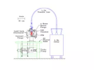
Hardware • Need: • Micro-electrode structure • Low T low energy electron source • Means to read out the states of the electrons • Microwave source
Micro-electrodes 15 mm square chip. Ground plane will cover only the lead wires of the left and right triangles. Thickness gauge capacitors Location of microelectrodes and leads to be written by ebeam lithography
Original pattern of two rows of posts separation = 500 nm • Ebeam lithography is independent of the photolithography lead pattern and can be changed from the original 2 row pattern.
Electron source • Porous silicon diode prepared by anodization in HF-water ethanol solution of n+ doped Si, 30mA/cm2, illuminated with 30 mW/cm2, 5 m RTO, 0.5 m anneal in N2 (to be published). • Yields as a few as 50 electrons per pulse with energies less than 10 eV. • Operating parameters are independent of T below ~ 1 K • Energy dissipation is negligible
0.80 0.75 Porous Si n+Si 4 0.70 x10 Au Au PS 0 V /I 0.65 E I Vbias - e VPS - e 0.60 collector HP33120A Signal Generator 2 3 4 5 6 7 8 9 10 1/f (msec) Electrometer IPS ~ VPS VE Schematic of experimental setup to measure properties of the PS diode. Individual pulses from the HP33120A of the form shown are applied. The frequency setting of the generator determines the slope of the sawtooth. The frequency dependence of the efficiency of production of emission current, IE . IPS (mA) VPS (V)
Superconducting microbolometers Tests with short wire, 1 m by 40 by150 nm thick Aluminum (shown without ground plane) · Three TC’s corresponding to transitions of the three different lead widths · Operated only close to TC = 1.2K · Resistance pulse height is fixed, width (duration) depends on energy · Total number of electrons in area of detector less than one per pulse so that only a fraction of pulses cause change in resistance · Field configuration was incorrect for 100% efficiency (alignment too critical). New meander pattern described below. Detectors
Meander pattern The meander pattern is calculated to give 100% detection efficiency with a misalignment as large as 1 mm. R=5 k. Holes through the chip between meander patterns to allow electrons to pass from the source to the microelectrodes. Edges of the meander pattern and the ground plane. 1.5 cm square chip with 1 mm square opening in the ground plane at the center.
Single electron detection with Ti meander Raw and filtered data from a resistance change caused by electron impact. The decay is the electronic time constant of the AC coupled signal. Resistance transitions due to electron impacts from pulses of ~55 electrons/ mm2 at 1 second intervals. Lower TC by ion implantation in Ti or W.
tunnel diode electron source transition edge detectors lower plate Schematic of the system micro-structure liquid He film